



Previous
Next
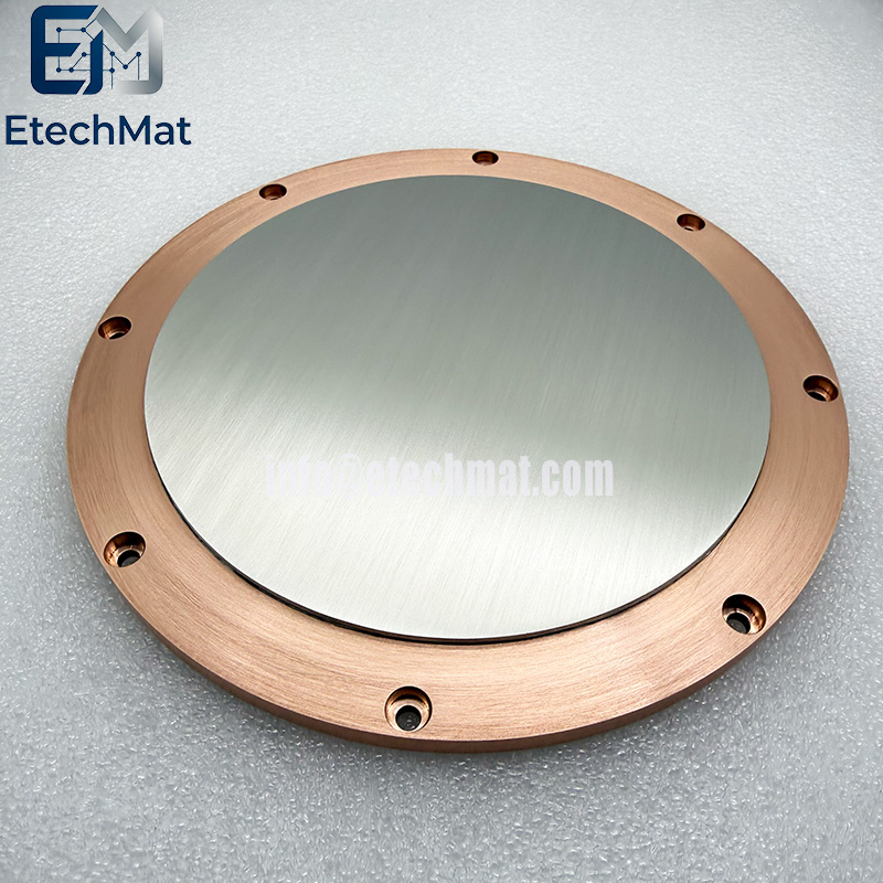
Tin Sputtering Target
Description of Tin Sputtering Target
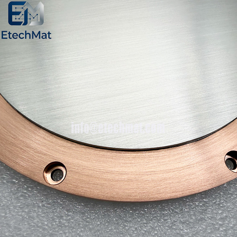
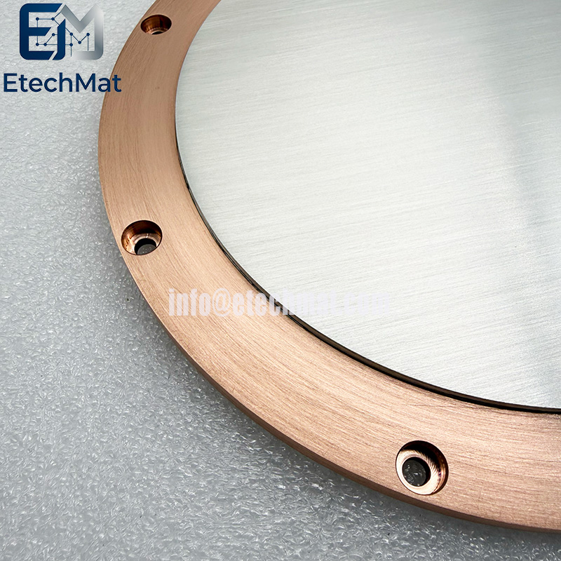
Tin is a practical metallic sputter source widely deployed for creating solder‑compatible and conductive thin films within vacuum deposition workflows. Its relatively low melting point creates real operational hurdles; inconsistent internal grain distribution can trigger hot spots, bringing uneven erosion and fluctuating film quality throughout long sputter cycles. Our tin sputtering target is fabricated from high‑purity feedstock with carefully tuned grain characteristics. It produces adherent, uniform tin layers suited for electronic contact structures, solderable surface finishes, and diverse material‑science research work. Each target goes through strict dimensional checks and surface quality evaluation before packing. Compatible with laboratory‑scale sputter chambers as well as pilot coating lines. Stable material performance reduces unexpected coating deviations, helping you achieve repeatable experimental results when developing electronic components and advanced thin‑film solutions.
Features of Tin Sputtering Target
1. High-purity tin for consistent thin films
2. Dense target for reduced arcing
3. Ideal for TCO and solder layers
4. Excellent uniformity for optical coatings
5. Custom sizes for all sputter systems
6. Low impurity for electronic applications
7. Suitable for DC and RF sputtering
8. Supplied with full material certification
9. Vacuum-sealed for oxidation prevention
10. Quick delivery for R&D projects
Applications of Tin Sputtering Target
In semiconductor manufacturing, they fabricate key chip structures including metal interconnects and barrier layers for integrated circuit production. For display panels, they cooperate with ITO targets to form transparent conductive films and electrodes for LCD and OLED displays. In the photovoltaic industry, they manufacture solar cell electrodes and back electrodes to boost photoelectric conversion efficiency. They also work with zinc-tin targets to deposit functional coatings for Low-E glass. Additionally, these targets support the production of optical, anti-corrosion, and other functional films for various electronic and optical devices.
Specifications of Tin Sputtering Target
Circular Sputtering Targets(Diameter): 1.0”2.0”3.0”4.0”5.0”6.0” up to 21”
Rectangular Sputtering Targets(Width x Length): 5” x 12”5” x 15”5” x 20”5” x 22”6” x 20”
Thickness: 0.125”, 0.25”
Shape: Disc/Rectangular/Tube
Bonding: Unbonding/Bonding
Purity: 2N(99%), 3N5(99.95%), 4N(99.99%), 4N5(99.995%),5N(99.999%).6N(99.9999%).
Process Highlights
Sputtering Method: Magnetron sputtering is typically employed. Tin can be sputtered using a pure metal target, or reactive sputtering—involving the introduction of oxygen or nitrogen—can be used to produce compound thin films (such as tin oxide).
Key Parameters: Target purity, density, grain size, and compositional uniformity directly influence the thin film's electrical conductivity, optical properties, and uniformity.
⚠️ Precautions
High-purity tin targets are subject to strict limits regarding impurities (especially radioactive elements), as these can become major sources of contamination in the thin film.
The process window must be carefully controlled during sputtering to prevent issues such as target poisoning, which can lead to reduced deposition rates and deviations in film composition.


