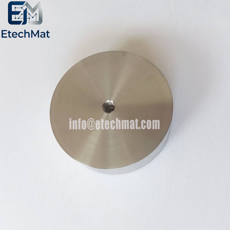
Sputtering targets are evolving toward larger sizes and higher purity.
High-purity metal sputtering targets are primarily used in wafer fabrication and advanced packaging processes. Taking chip manufacturing as an example, the transformation from a silicon wafer into a finished chip involves seven major production stages: thermal processing (diffusion), photolithography, etching, ion implantation, dielectric deposition (thin-film growth), chemical mechanical polishing (CMP), and metallization. Each stage relies on specific equipment, materials, and processes. Sputtering targets are utilized during the "metallization" phase; thin-film deposition equipment bombards the target with high-energy particles to form functional metal layers—such as conductive or barrier layers—on the silicon wafer. As technological advancements occur in downstream markets regarding thin-film products and components, sputtering target technology must evolve in tandem. Among downstream sectors, the semiconductor industry imposes the most rigorous quality standards for sputtering targets and sputtered films. The production of larger silicon wafers necessitates a shift toward larger sputtering targets and demands stricter control over grain size and crystallographic orientation. Since the purity of the sputtered film is directly tied to that of the target, the demand for higher precision and finer micron-scale semiconductor processes has steadily driven the required purity of sputtering targets upward, reaching 99.9999% (6N) or higher.