



Previous
Next
Te Tellurium 99.99% Pure Sputtering Target
Description of Te Tellurium 99.99% Pure Sputtering Target
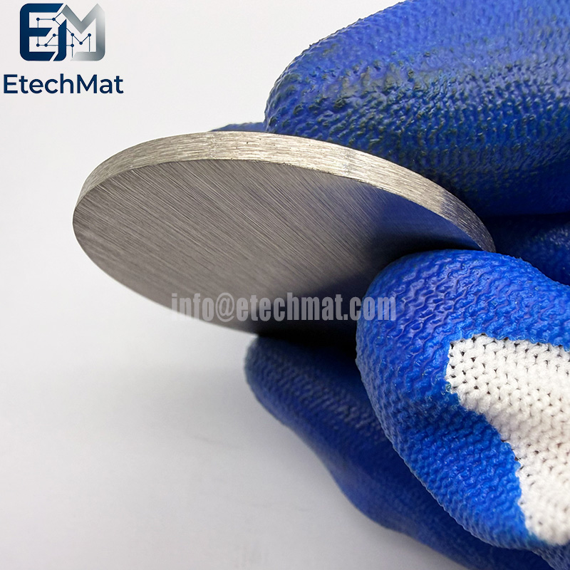
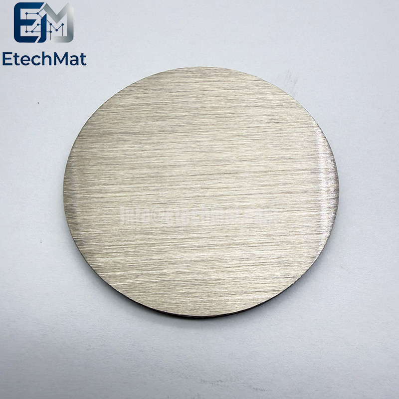
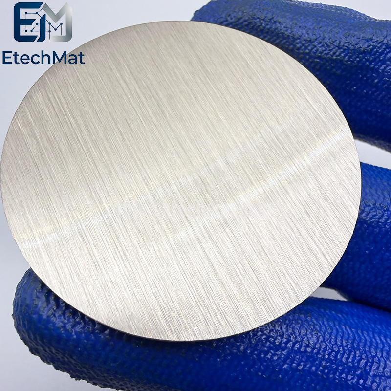
Our 99.99% Pure Te Tellurium Sputtering Target tackles the well-known volatility challenge of elemental tellurium. Many standard tellurium targets suffer from uneven grain distribution. During sputtering, excessive Te outgassing causes fluctuating deposition rates, rough film surfaces, and inconsistent results for your thermoelectric, phase-change, and topological insulator studies. We use high-grade 4N tellurium raw material and optimized forming processes to create a dense, uniform target body. The refined microstructure helps moderate volatile Te release, stabilizing deposition and lowering particle defects. It is widely used for preparing thermoelectric layers, phase-change memory films, and quantum material thin films. Each target passes strict purity and surface inspection before shipment. Standard sizes are available, and backing plate bonding service can be arranged for reliable vacuum chamber operation. Custom shapes and dimensions are also offered to match your PVD system. Cut down wasted substrates from unstable tellurium flux and spend more time collecting repeatable experimental data for your material research.
Features of Te Tellurium 99.99% Pure Sputtering Target
99.99% ultra-high purity can effectively avoid unstable glow discharge caused by impurities, significantly reduce the defect rate of thin film particles, and ensure the electrical performance and yield of devices.
Fine crystal uniform microstructure, stable and controllable sputtering rate, excellent uniformity of film thickness, suitable for batch coating requirements of large-sized substrates.
The low melting point characteristic allows for lower sputtering deposition temperatures, making it suitable for special coating scenarios such as flexible substrates and thermosensitive substrates.
A high-purity, dense structure can significantly reduce abnormal ignition and particle splashing during the sputtering process, prolong the service life of the target material, and reduce the maintenance cost of the coating process.
Applications of Te Tellurium 99.99% Pure Sputtering Target
In the field of photovoltaic energy, it is used for the deposition of absorption layers in cadmium telluride thin film solar cells. The purity and uniformity of the target material directly determine the photovoltaic conversion efficiency of the cell.
Semiconductor manufacturing: deposition of tellurium-containing functional thin films for chip interconnect layers, phase change memory, and topological quantum devices. It is a core source material for advanced storage and quantum material research.
In the field of flat displays, special optical anti-reflective films and electrode layer preparation are used for OLED panels to optimize panel transmittance and conductivity.
Special coatings and scientific research: widely applicable to magnetron sputtering systems in various universities and research institutes, used for the preparation and research of cutting-edge thin films such as two-dimensional magnetic materials and topological insulators.
Specifications of Te Tellurium 99.99% Pure Sputtering Target
Circular Sputtering Targets (Diameter): 1.0”, 2.0”, 3.0”, 4.0”, 5.0”, 6.0”, up to 12”
Rectangular Sputtering Targets (Width x Length): 5” x 12”, 5” x 15”, 5” x 20”
Thickness: 0.125”, 0.25”
Shape: Disc/Rectangular
Bonding: Unbonded/Bonded
Purity: 4N (99.99%)


