



Previous
Next
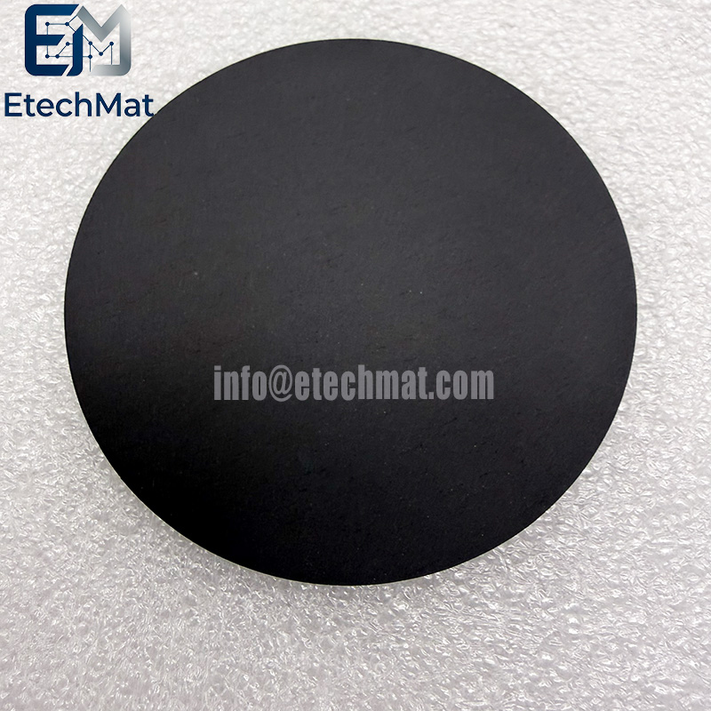
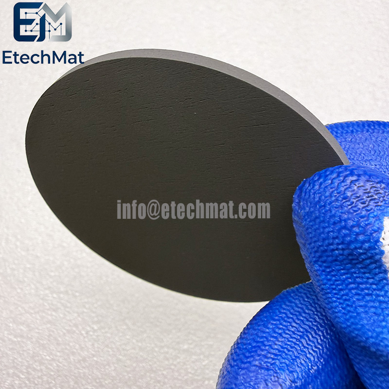
Pure B Boron Sputter Target
Description of Pure B Boron Sputter Target
Pure boron is a niche yet critical material for specialty thin‑film deposition, widely used for doping and neutron‑responsive functional layers. Pure boron is inherently difficult to densify; residual pores and loose grain boundaries frequently cause particle spitting during sputtering, contaminating substrates and ruining batch‑to‑batch experimental consistency. Our pure B boron sputter target is consolidated under optimised conditions to reduce internal porosity and achieve homogeneous microstructure. It generates high‑purity, low‑contamination boron thin‑films well‑suited for semiconductor doping processes and advanced neutron‑related coating research. Every unit undergoes dimensional verification, microstructure sampling, and strict surface inspection before dispatch. Compatible with laboratory and pilot‑scale sputtering hardware. Its improved structural stability suppresses particle defects, helping you maintain reliable, repeatable coating outcomes for your high‑spec thin‑film development work.
Features of Pure B Boron Sputter Target
1. Pure boron for high‑purity thin films
2. Dense target for stable deposition rates
3. Excellent uniformity for optical coatings
4. Ideal for semiconductor doping applications
5. Custom sizes for R&D and production
6. Low impurity for consistent device performance
7. Suitable for RF and DC magnetron systems
8. Supplied with purity and density certificates
9. Vacuum‑sealed for contamination‑free use
10. Reliable performance for neutron detection
Applications of Pure B Boron Sputter Target
Semiconductor industry: Used for silicon doping to change the electrical properties of semiconductor materials; it is a key consumable in chip manufacturing.
Optoelectronic technology: As the basic material of optical thin films, it is used to manufacture various optical devices.
Nuclear industry and biomedicine: Utilizing the neutron absorption capacity of boron for nuclear reactor control materials; In radioactive isotope applications such as boron neutron capture therapy (BNCT), it can be used for targeted therapy of tumor cells.
Scientific research experiments: widely used in thin film preparation experiments such as magnetron sputtering and plasma deposition, suitable for DC/RF sputtering systems.
Specifications of Pure B Boron Sputter Target
Circular Sputtering Targets(Diameter): 1.0”2.0”3.0”4.0”5.0”6.0” up to 21”
Rectangular Sputtering Targets(Width x Length): 5” x 12”5” x 15”5” x 20”5” x 22”6” x 20”
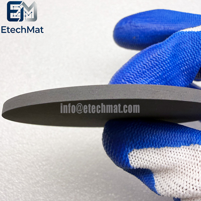
Thickness: 0.125”, 0.25”
Shape: Disc/Rectangular
Bonding: Unbonding/Bonding
Purity: 2N(99%), 3N5(99.95%), 4N(99.99%), 4N5(99.995%),5N(99.999%).
Production Process
Preparation Process: Purification and shaping are typically achieved through methods such as electron beam (EB) melting, vacuum arc remelting (VAR), or spark plasma sintering (SPS). The material then undergoes precision machining to form the target, ensuring high density and uniform grain structure.
⚠️ Precautions
Storage: Packaging under inert gas or proper storage is recommended to prevent oxidation and maintain sputtering performance.
Selection Factors: Parameters such as target purity, dimensions, density, and grain size should be comprehensively considered based on the coating equipment, required thin-film properties, and budget.


