



Previous
Next
High Purity Bi Bismuth Sputtering Target
Description of High Purity Bi Bismuth Sputtering Target
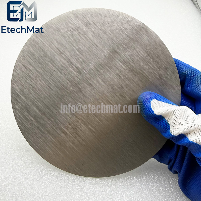
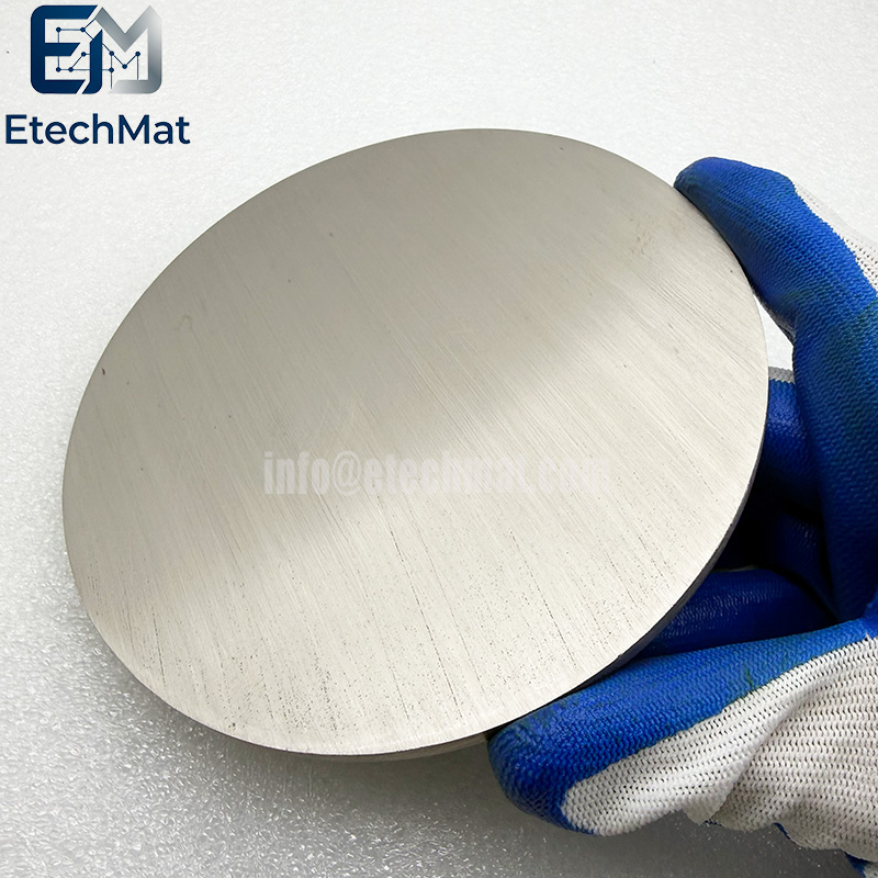
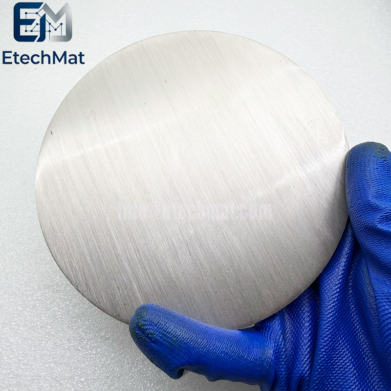
High-Purity Bi Bismuth Sputtering Target is developed for thin-film processes where material consistency matters as much as nominal purity. Using high-purity bismuth, it provides a dependable material source for semiconductor research, electronic devices, optical applications, and the development of bismuth-based functional films. For many deposition processes, unexpected changes in target composition or surface condition can translate into unstable deposition rates, inconsistent film properties, and difficult-to-repeat experimental results. This bismuth sputtering target is manufactured with controlled material quality and uniform composition to help reduce these variables and give engineers better control over their deposition process. Rather than focusing on a purity number alone, the target is designed around practical sputtering requirements, including stable operation, consistent material behavior, and compatibility with different PVD and magnetron sputtering systems. This makes it suitable for both laboratory-scale research and applications requiring repeatable thin-film preparation. High Purity Bi Bismuth Sputtering Target is available in customized dimensions, shapes, and configurations to match specific equipment and process requirements. For customers working with bismuth thin films, it offers a straightforward way to reduce material-related uncertainty and keep deposition results more consistent from batch to batch.
Features of High Purity Bi Bismuth Sputtering Target
Material Properties: Bismuth has an atomic number of 83 and exhibits intrinsic characteristics such as extremely low thermal conductivity, a significant Hall effect, strong spin-orbit coupling, and substantial room-temperature carrier mobility. These properties enable the formation of nanoscale thin films with controllable lattice distortion and abundant surface states during the sputtering process.
Specifications and Forms: Targets can be manufactured in circular (e.g., 2-inch, 3-inch, 4-inch) or square shapes, with dimensions customizable to specific requirements. Purity levels include 4N and 5N grades, and surfaces typically undergo polishing or grinding treatments.
Applications of High Purity Bi Bismuth Sputtering Target
Optical Thin Films: Used to prepare transparent conductive films for optoelectronic devices such as photovoltaic cells and displays.
Electronic Devices: Due to its high mobility and low resistivity, bismuth is suitable for manufacturing high-mobility field-effect transistors (TFTs), magnetic memory materials, and sensors.
Magnetic Materials: Bismuth thin films sputtered onto magnetic substrates can exhibit ferromagnetic properties, making them applicable to magnetic storage technologies.
Flexible Electronics: Bismuth thin films on polyimide (PI) or PET substrates can form micro-wrinkled buffer structures; the sheet resistance changes by only 3.2% after 200,000 bending cycles, outperforming traditional ITO-based solutions.
Optoelectronic Devices: In perovskite solar cells and OLEDs, bismuth thin films serve as synergistic interfaces for photon management and carrier injection; when replacing MoO₃ as the hole transport layer, the open-circuit voltage can increase by 120 mV.
Quantum Manipulation: Hetero-interfaces formed with ferromagnetic metals or topological insulators can induce Rashba splitting, enabling applications in spintronic chips and non-volatile memory.
Specifications of High Purity Bi Bismuth Sputtering Target
Circular Sputtering Targets (Diameter): 1.0”, 2.0”, 3.0”, 4.0”, 5.0”, 6.0”, up to 12”
Rectangular Sputtering Targets (Width x Length): 5” x 12”, 5” x 15”, 5” x 20”, 5” x 22”, 6” x 20”
Thickness: 0.125”, 0.25”
Shape: Disc/Rectangular
Bonding: Unbonded/Bonded
Purity: 4N(99.99%)


