



Previous
Next
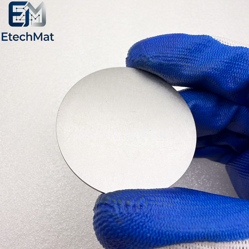
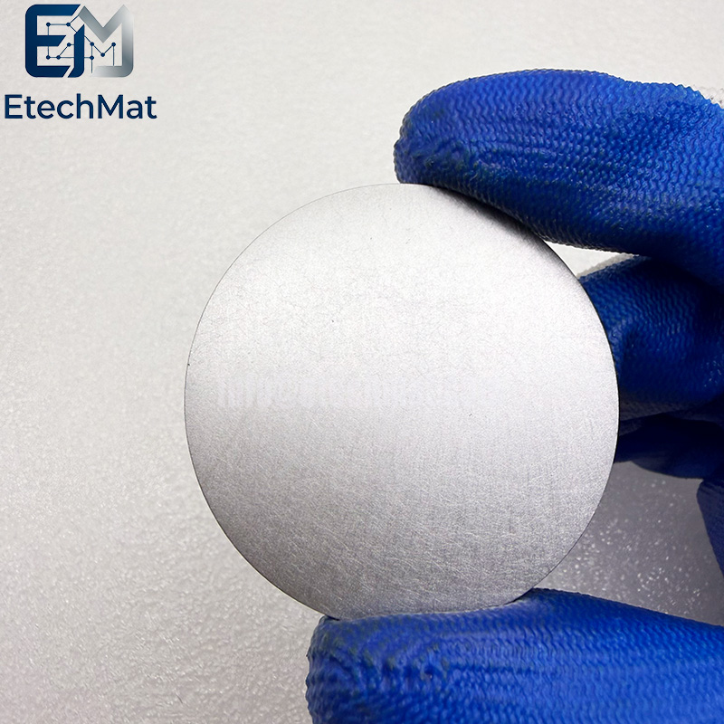
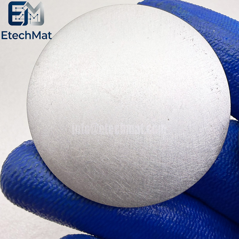
Fe Iron 99.99% Pure Sputter Target
Description of Fe Iron 99.99% Pure Sputter Target
Our 99.99% Pure Fe Iron Sputter Target addresses recurring experimental headaches brought on by lower‑purity iron targets. Extraneous trace contaminants and erratic grain structures often trigger sputtering‑rate instability, poor film homogeneity, and distorted magnetic measurement data that waste precious lab time and sample substrates. High‑grade raw feedstock goes through precision forming and tailored heat treatment to achieve evenly distributed grain morphology across the entire target body, keeping impurity levels tightly constrained. It delivers steady sputtering performance run‑to‑run, well‑suited for magnetic material research, multi‑element alloy thin‑film fabrication, and lab‑scale semiconductor‑related development. Every target passes strict quality validation before shipment. A broad selection of standard sizes is available, and backing‑plate bonding service supports straightforward chamber mounting. Custom geometries can be manufactured for non‑standard experimental hardware. Minimise frustrating trial‑and‑error cycles caused by defective iron films, allowing you to focus your resources on advancing your material‑science research goals.
Features of Fe Iron 99.99% Pure Sputter Target
1. 99.99% pure iron for sputtering
2. High-purity Fe for advanced films
3. Excellent magnetic properties for storage
4. Dense target for stable deposition
5. Ideal for magnetic recording layers
6. Custom sizes for R&D systems
7. Low impurity for device-grade quality
8. Suitable for DC and RF magnetron
9. Supplied with purity certificate
10. Vacuum-sealed to prevent oxidation
Applications of Fe Iron 99.99% Pure Sputter Target
Magnetic storage and spintronics: Iron thin films are the core functional layers of devices such as giant magnetoresistance (GMR) multilayers and magnetic random access memory (MRAM), directly affecting data read and write performance.
Semiconductors and Microelectronics: Can be used for copper interconnect barrier layers (such as FeN, FeTaN), electrode materials, etc., and can also be used for coating in fields such as solar photovoltaics and flat displays.
Research and Basic Research: Suitable for various single-target and multi-target sputtering systems, commonly used in materials science research, micro-nano processing, and device fabrication.
Specifications of Fe Iron 99.99% Pure Sputter Target
Circular Sputtering Targets(Diameter): 1.0”2.0”3.0”4.0”5.0”6.0” up to 21”
Rectangular Sputtering Targets(Width x Length): 5” x 12”5” x 15”5” x 20”5” x 22”6” x 20”
Thickness: 0.125”, 0.25”
Shape: Disc/Rectangular
Bonding: Unbonding/Bonding
Purity: 4N(99.99%).


