



Previous
Next
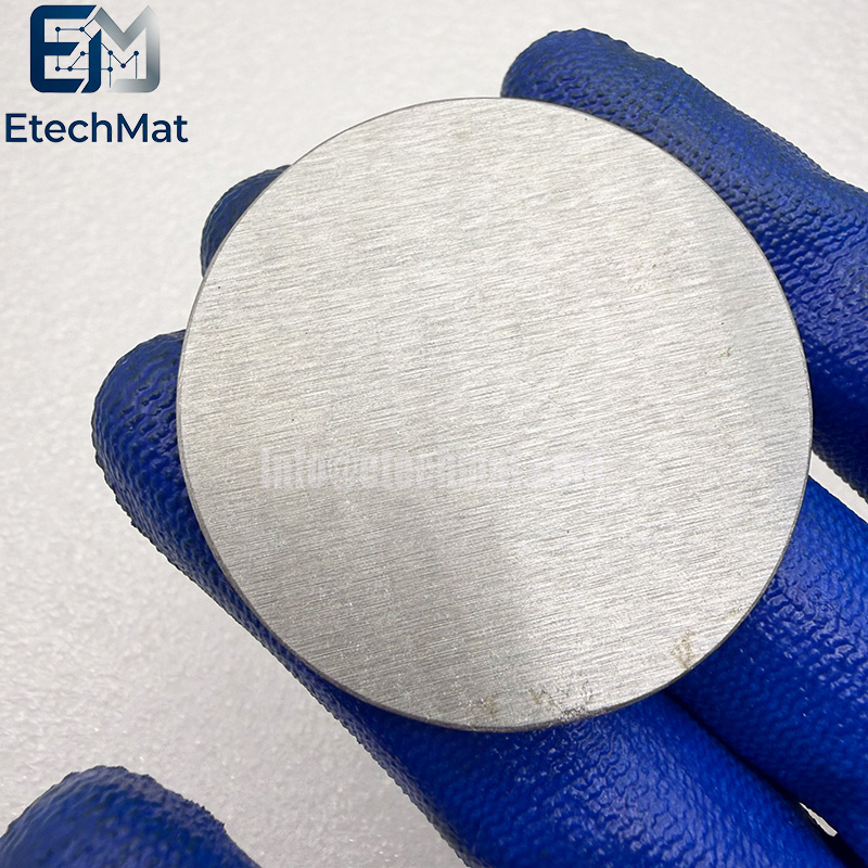
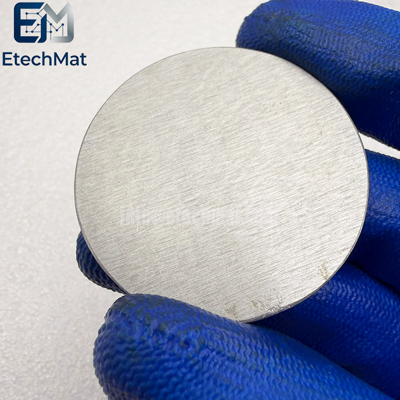
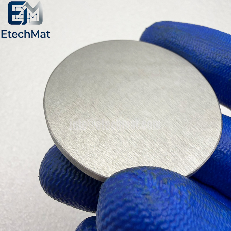
4N Bi Bismuth Sputtering Target
Description of 4N Bi Bismuth Sputtering Target
Our 4N Bi Bismuth sputtering target addresses common difficulties for thermoelectric and low‑temperature thin‑film work. Ordinary bismuth targets often show uneven grain distribution and easy oxidation, leading to unstable film composition and poor repeatability in your trials. We use high‑purity raw bismuth and optimized forming processes to create a dense, homogeneous target. Controlled grain structure reduces segregation and surface oxidation, supporting steady deposition for thermoelectric layers and superconducting device research. Every target gets purity and surface inspection before shipment. Standard sizes are ready, and backing bonding service is available for stable chamber runs. Custom shapes and dimensions can be made to fit your sputtering system. Cut down wasted samples from inconsistent bismuth films, so you can focus on gathering reliable electrical and thermal measurement data for your R&D.
Features of 4N Bi Bismuth Sputtering Target
1. 4N bismuth for high‑purity films
2. Dense Bi target for stable sputtering
3. Ideal for topological insulator research
4. Excellent thermoelectric properties for devices
5. Custom sizes for R&D systems
6. Low impurity for consistent performance
7. Suitable for DC and RF magnetron
8. Supplied with purity analysis certificate
9. Vacuum‑sealed for oxidation prevention
10. Reliable quality for advanced applications
Applications of 4N Bi Bismuth Sputtering Target
Semiconductors and Electronics: Used for thin-film deposition in chip manufacturing; advanced processes have a specific demand for high-purity bismuth sputtering targets.
Thermoelectric Energy Conversion: Bismuth exhibits a high Seebeck coefficient of up to -100 μV/K (n-type) and a strong thermoelectric effect, capable of converting minute temperature differences into voltage; it is a key component of high-performance thermoelectric materials.
Optics and Flexible Electronics: Its low-temperature deposition characteristics make it suitable for preparing thin films on flexible substrates; it is also used for optical coatings.
Scientific Research: Widely used in experimental research within fields such as high-energy physics and materials science.
Specifications of 4N Bi Bismuth Sputtering Target
Circular Sputtering Targets (Diameter): 1.0”, 2.0”, 3.0”, 4.0”, 5.0”, 6.0” up to 21”
Rectangular Sputtering Targets (Width x Length): 5” x 12”, 5” x 15”, 5” x 20”, 5” x 22”, 6” x 20”
Thickness: 0.125”, 0.25”
Shape: Disc/Rectangular
Bonding: Unbonded/Bonded
Purity: 4N (99.99%)
Difficulties in the preparation of 4N Bi Bismuth Sputtering Target
Bismuth expands by about 3.3% in volume during solidification, and due to its extreme brittleness and significant anisotropy in thermal expansion, it is prone to cracking or porosity during casting. Therefore, special processes such as low-temperature precision casting and multi-stage annealing are required to control internal stress. In addition, bismuth has a low melting point, and attention should be paid to the thermal management of the target surface during high-power sputtering to avoid local softening or even melting.


