



Previous
Next
3N5 W Tungsten Sputtering Target
Description of 3N5 W Tungsten Sputtering Target
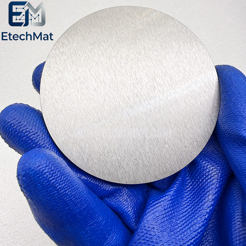
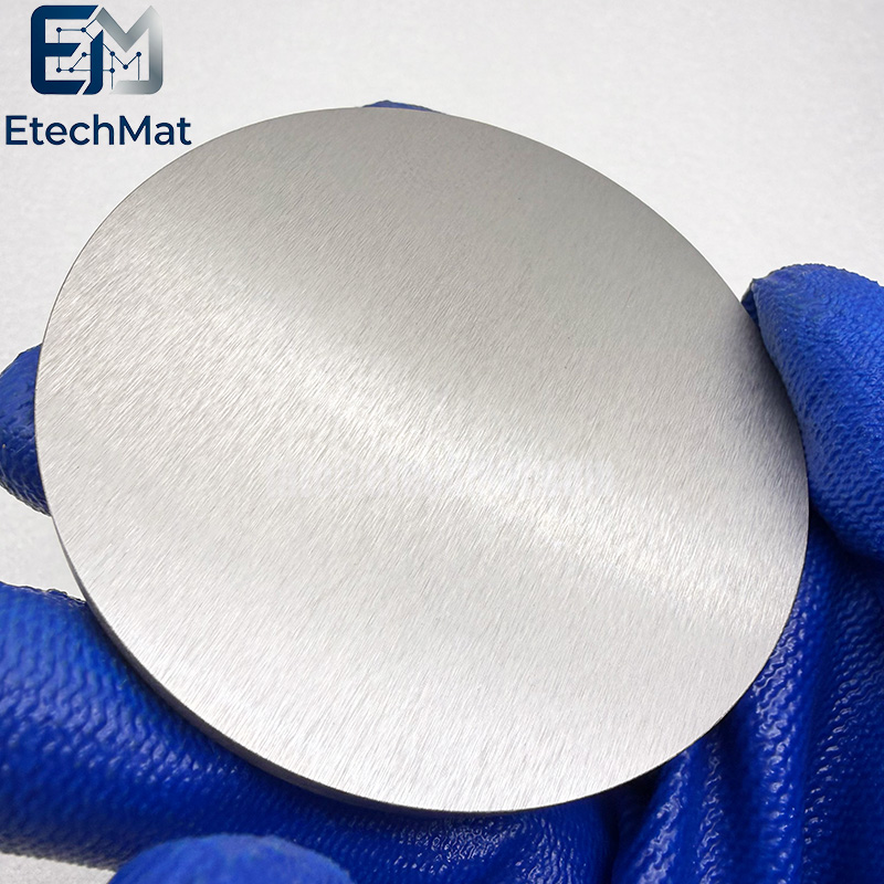
Tungsten is favoured for sputtering work thanks to its outstanding melting‑point performance and good chemical stability. Even minor material defects, such as residual impurities or poorly consolidated inner structures, may create hot spots during long‑time sputtering runs. This brings irregular target erosion and disturbs the consistency of deposited metallic thin‑films for precision laboratory projects. Our 3N5 W tungsten sputtering target is processed from 3N5 high‑purity raw tungsten. Advanced powder metallurgy processes deliver well‑homogenised grain structure and low impurity content across the target surface. It produces dependable tungsten thin‑films for semiconductor barrier structures, high‑temperature protective layers and various material‑science R‑D tasks. Each target undergoes impurity screening, dimensional testing and careful surface inspection before shipment. Optimised for standard magnetron sputtering cathodes used in labs and pilot facilities. Stable material behaviour reduces unexpected hot‑spot risks, supporting consistent thin‑film performance throughout your coating development cycles.
Features of 3N5 W Tungsten Sputtering Target
1. 3N5 tungsten for high-purity films
2. Excellent thermal stability for sputtering
3. Dense target for uniform deposition
4. Ideal for semiconductor barrier layers
5. Custom sizes for R&D systems
6. Low impurity for device-grade quality
7. Suitable for DC magnetron sputtering
8. Supplied with purity certificate
9. Vacuum-sealed for oxidation prevention
10. Reliable performance for electronic coatings
Applications of 3N5 W Tungsten Sputtering Target
Semiconductors and Microelectronics: Tungsten layers are integral components of thin-film transistors (TFTs) in TFT-LCD screens and serve as diffusion barriers and conductive interconnects in the microelectronics industry, frequently utilized in contact hole processes for logic devices and memory chips.
Thin-Film Deposition Quality: High-purity targets enable the deposition of thin films with excellent conductivity and minimal particulate contamination during PVD processes, thereby preventing circuit shorts or damage.
Specifications of 3N5 W Tungsten Sputtering Target
Circular Sputtering Targets(Diameter): 1.0”2.0”3.0”4.0”5.0”6.0” up to 21”
Rectangular Sputtering Targets(Width x Length): 5” x 12”5” x 15”5” x 20”5” x 22”6” x 20”
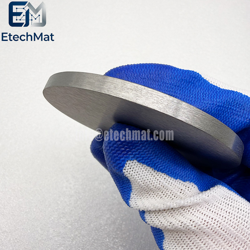
Thickness: 0.125”, 0.25”
Shape: Disc/Rectangular/Tube
Bonding: Unbonding/Bonding
Purity: 2N(99%), 3N(99.9%), 3N5(99.95%).


