



Previous
Next
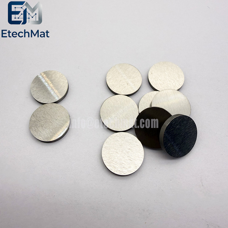
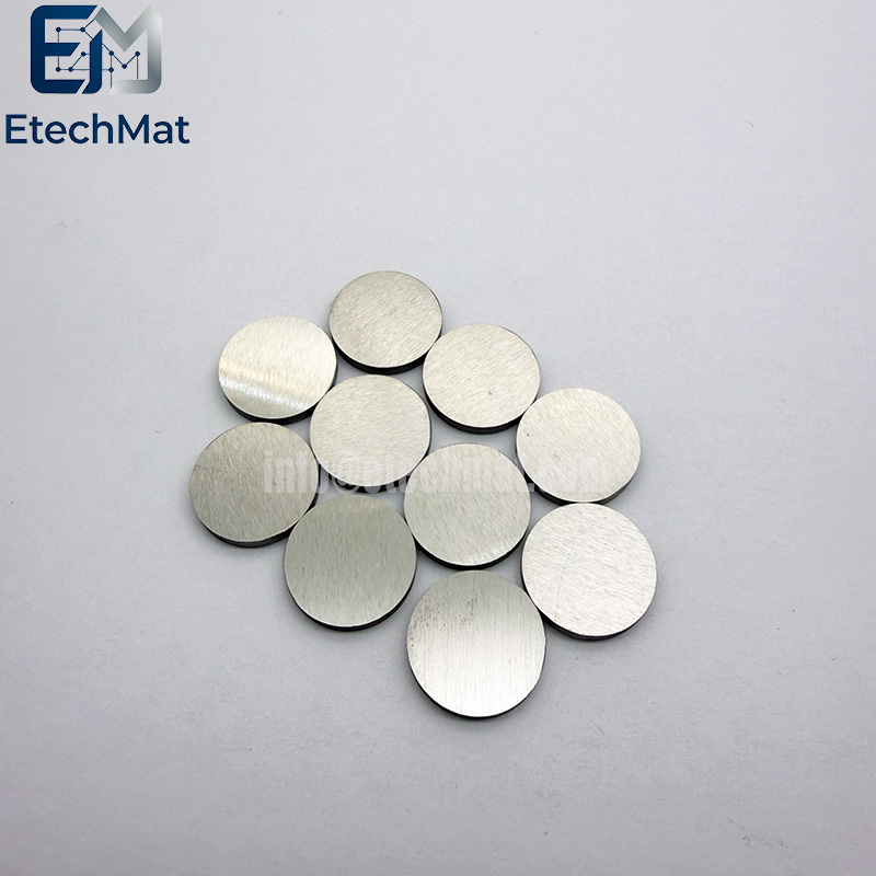
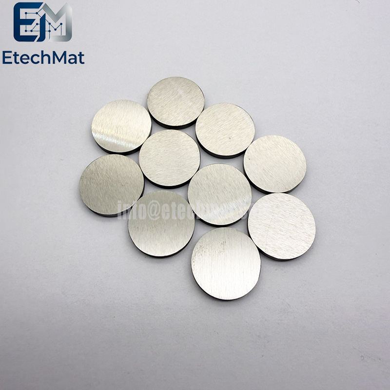
3N5 W Tungsten Sputter Target
Description of 3N5 W Tungsten Sputter Target
3N5 W Tungsten Sputter Target is developed for manufacturers seeking a balance between material reliability, deposition consistency, and production efficiency. Made from tungsten with a purity level of 99.95%, it offers stable sputtering performance and uniform film formation for applications such as semiconductor components, optical coatings, electronic devices, and advanced surface treatments. In real production environments, material consistency directly affects yield, equipment stability, and overall process costs. This tungsten sputter target is designed to help reduce common issues such as uneven deposition, unnecessary target replacement, and process interruptions. Its controlled microstructure, excellent thermal conductivity, and dependable sputtering characteristics support long-duration operation with repeatable results. Available in various sizes and configurations, 3N5 W Tungsten Sputter Target can be customized to meet different equipment requirements and application conditions. With strict quality inspection from raw material selection to final processing, it provides a practical solution for customers who need reliable tungsten targets without compromising production performance.
Features of 3N5 W Tungsten Sputter Target
1. Features an ultra-high melting point and thermal stability; the target undergoes virtually no thermal deformation during sputtering, enabling prolonged, continuous operation.
2. High density and compactness ensure a stable sputtering process, effectively reducing particle splashing and guaranteeing the uniformity of the deposited thin film.
3. Excellent electrical and thermal conductivity make it suitable for DC magnetron sputtering processes, offering high deposition rates and good process repeatability.
4. Chemically extremely stable; it does not react with the vast majority of acids or alkalis at room temperature, resulting in thin films with excellent corrosion and oxidation resistance.
5. Compared to 6N-grade semiconductor-grade ultra-high-purity tungsten targets, the 3N5-grade product offers superior cost-effectiveness, significantly reducing consumable costs in industrial coating applications.
Applications of 3N5 W Tungsten Sputter Target
Semiconductors and Microelectronics: As a key component of thin-film transistors (TFTs) in TFT-LCD screens, tungsten layers remain extremely stable in high-temperature environments; they also serve as diffusion barriers and conductive interconnects in microelectronics.
Advanced Memory Chips: Ultra-high-purity tungsten targets are critical materials for manufacturing advanced memory chips. Industry data from June 2026 indicates that only a few leading enterprises—such as Kingsemi (Jiangfeng Electronics)—possess the core technology for their mass production.
Solar Cells: Used to fabricate conductive layers and electrodes.
Optical Coatings: Suitable for precision coating applications, such as anti-reflective coatings for optical lenses.
Specifications of 3N5 W Tungsten Sputter Target
Circular Sputtering Targets (Diameter): 1.0”, 2.0”, 3.0”, 4.0”, 5.0”, 6.0”, up to 12”
Rectangular Sputtering Targets (Width x Length): 5” x 12”, 5” x 15”, 5” x 20”
Thickness: 0.125”, 0.25”
Shape: Disc/Rectangular
Bonding: Unbonded/Bonded
Purity: 3N5 (99.95%)
⚠️ Precautions
Pure tungsten is usually brittle and difficult to process, but high-purity tungsten can maintain hardness and have sufficient ductility for processing.
The purity of the target material directly affects the conductivity and particle defects of the thin film. High-purity target materials can achieve more uniform film layers and faster sputtering rates.
Tungsten target materials have relatively poor conductivity and are inferior to titanium or copper target materials in applications that require high conductivity, and their preparation costs are relatively high.


