



Previous
Next
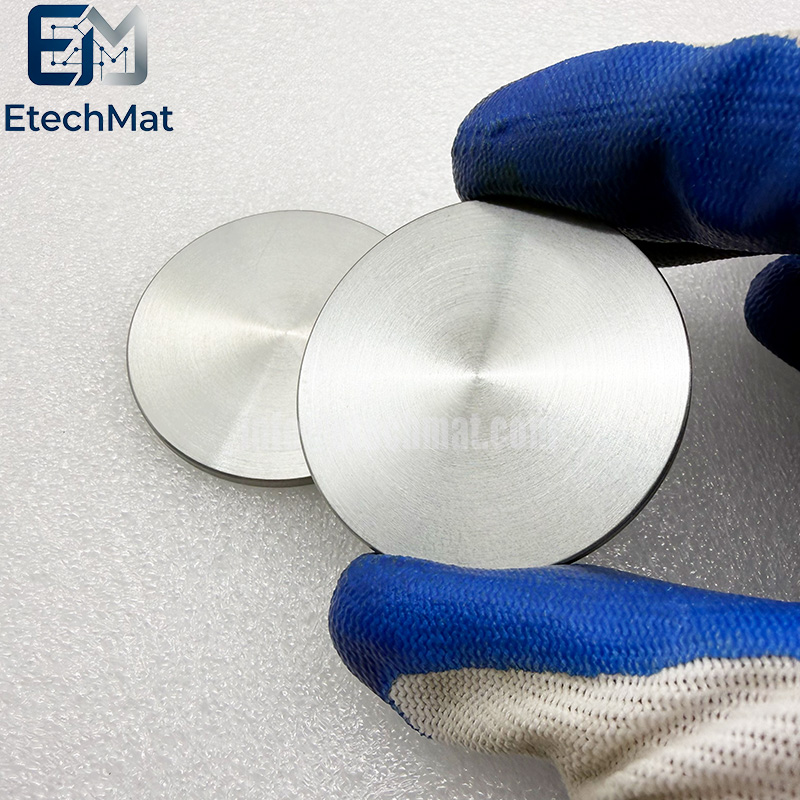
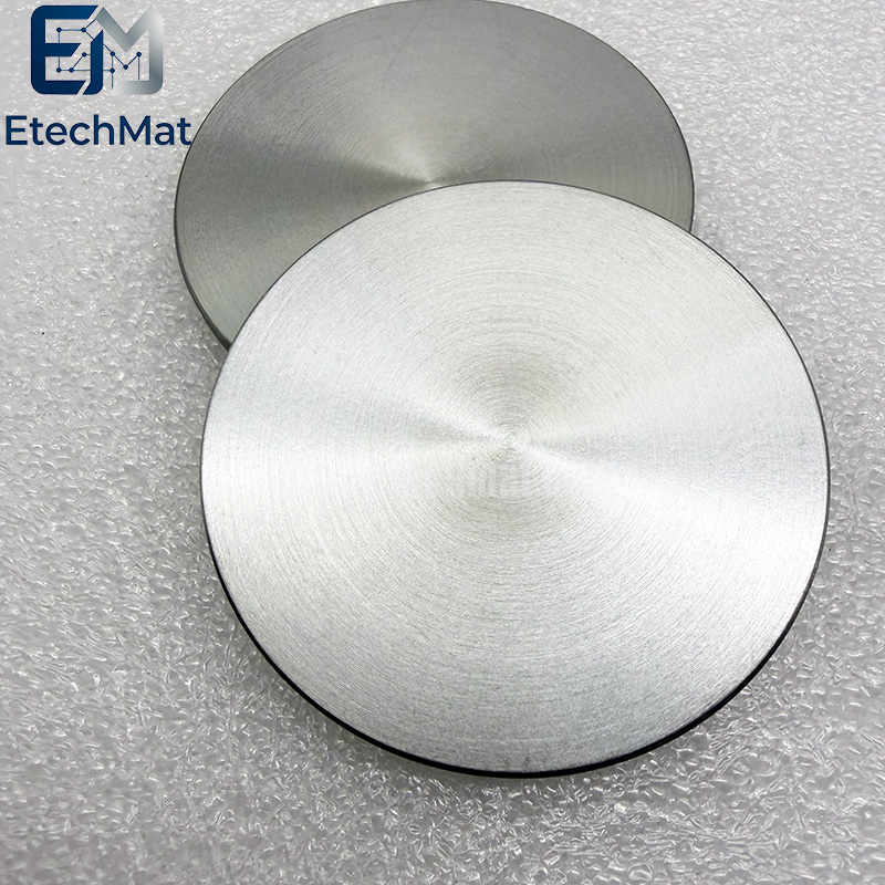
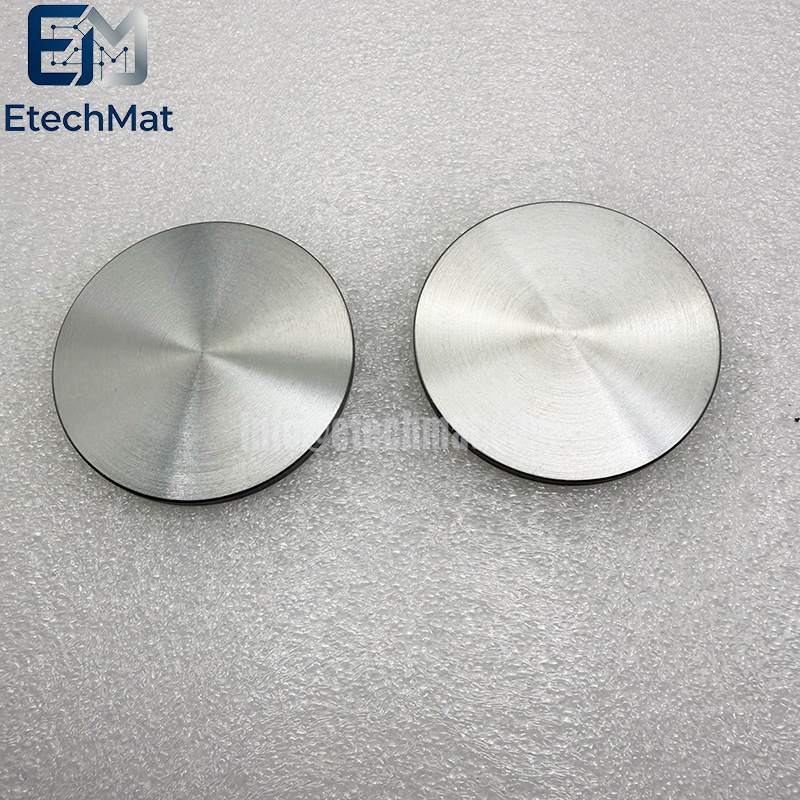
3N5 Hf Hafnium Wafer
Description of 3N5 Hf Hafnium Wafer
Our 3N5 Hf Hafnium Wafer tackles typical lab‑scale hurdles for high‑temperature and semiconductor research. Generic hafnium wafers often come with inconsistent surface quality, residual processing contaminants and uneven grain structures, which introduce unwanted noise during characterisation and compromise the reliability of your test results. Premium‑grade raw hafnium material undergoes precision cutting, fine grinding and tailored thermal processing to achieve homogeneous grain distribution, tightly controlled impurity levels and a clean, uniform surface finish. This well‑processed wafer fits thermal‑property testing, substrate‑based thin‑film growth and high‑temperature material‑related investigations. Each wafer receives strict dimensional and purity verification before delivery. Standard dimensions are readily accessible, and custom thicknesses or surface finishes can be tailored for your specific setup. Reduce misleading measurement artefacts from poorly processed hafnium substrates, freeing your lab resources to focus on generating trustworthy, repeatable material‑science data for your research work.
Features of 3N5 Hf Hafnium Wafer
1. 3N5 hafnium wafer for sputtering
2. High-purity Hf for advanced deposition
3. Excellent thermal stability for coatings
4. Ideal for semiconductor gate electrodes
5. Custom wafer sizes available
6. Dense structure for uniform erosion
7. Low impurity for device-grade films
8. Suitable for DC and RF magnetron
9. Supplied with purity certificate
10. Vacuum-sealed for oxidation protection
Applications of 3N5 Hf Hafnium Wafer
Advanced process gate dielectric: Starting from the 45nm node, Intel, TSMC, Samsung, and others use HfO ₂ as the gate insulation layer in the HKMG process.
New direction of ferroelectric storage: By doping elements such as Zr, Si, Al, etc., the ferroelectric orthogonal phase of hafnium oxide can be stabilized, which is used for new types of memory such as FeRAM and FeFET.
Sputtering target material: High-purity hafnium target material is used for physical vapor deposition (PVD) to form semiconductor or optical thin films.
Specifications of 3N5 Hf Hafnium Wafer
Circular Sputtering Targets(Diameter): 1.0”2.0”3.0”4.0”5.0”6.0” up to 21”
Rectangular Sputtering Targets(Width x Length): 5” x 12”5” x 15”5” x 20”5” x 22”6” x 20”
Thickness: 0.125”, 0.25”
Shape: Disc/Rectangular
Bonding: Unbonding/Bonding
Purity: 3N5(99.95%).
⚠️ Note
Hafnium materials require strict control of cross-contamination in wafer manufacturing - hafnium and zirconium are prone to introducing contamination in process solutions, especially in neutral or alkaline solutions such as ammonia-hydrogen peroxide mixtures. Cross-contamination between wafers in plasma etching equipment is also severe, requiring specialized cleaning procedures.


