



Previous
Next
ZrO2+2%Ti 99.99% Pure Sputter Target
Description of ZrO2+2%Ti 99.99% Pure Sputter Target
Our 99.99% pure ZrO₂+2%Ti sputter target is engineered to fix common pain points seen with standard zirconia targets, such as unexpected arcing, uneven sputtering rates, and inconsistent film quality that ruin your coating runs. The controlled 2 wt% titanium additive improves electrical conductivity throughout the target body, resulting in far more stable RF‑sputtering behaviour. We carefully optimise sintering processes to achieve homogeneous element distribution and low impurity content, so you avoid unexpected defects that skew your optical or optoelectronic test results. It works reliably for anti‑reflection layers, high‑reflection coatings and other functional dielectric thin‑film development. Whether you run lab‑scale R&D or small‑batch pilot production, this target keeps your deposition results reproducible batch‑to‑batch. Custom dimensions and bonding services are available to match your existing sputtering equipment, helping you cut down trial‑and‑error time in your workflow.
Features of ZrO2+2%Ti 99.99% Pure Sputter Target
High Purity: Target purity directly affects thin-film quality; high-end applications require ≥99.99% purity to prevent impurities from introducing electrical defects.
High Density and Uniformity: Density influences sputtering rates and film properties, with high-density targets better able to withstand thermal stress during sputtering; fine, uniform grains contribute to more uniform film thickness distribution.
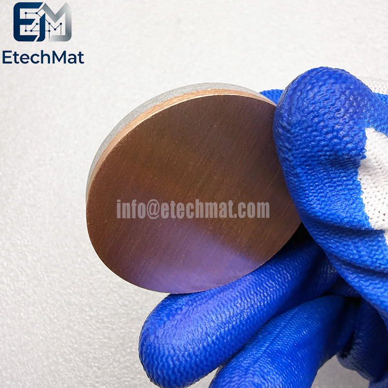
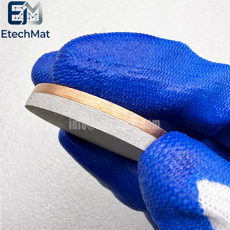
Brittleness and Thermal Conductivity: As a ceramic compound target, the ZrO₂ matrix is inherently brittle and has poor thermal conductivity, making it prone to cracking during prolonged, continuous sputtering; bonding to a copper backing plate is recommended to improve thermal conductivity and service life.
Applications of ZrO2+2%Ti 99.99% Pure Sputter Target
Semiconductors and integrated circuits: used for depositing high dielectric constant insulation layers or gate dielectrics to improve transistor performance.
Optical thin films and coatings: Sputtered thin films have high refractive index and hardness, and are used as anti-reflective or protective films for lenses and displays.
Optoelectronics and sensors: Deposition of zirconia layer on sensor components to improve anti-interference ability and accuracy.
Decoration and protective coating: can prepare interference colors, with high hardness and corrosion resistance, used for surfaces such as watches and mobile phone cases.
Specifications of ZrO2+2%Ti 99.99% Pure Sputter Target
Circular Sputtering Targets(Diameter): 1.0”2.0”3.0”4.0”5.0”6.0” up to 21”
Rectangular Sputtering Targets(Width x Length): 5” x 12”5” x 15”5” x 20”5” x 22”6” x 20”
Thickness: 0.125”, 0.25”
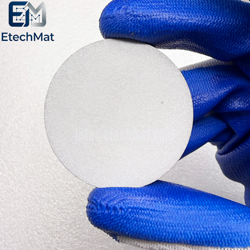
Shape: Disc/Rectangular
Bonding: Unbonding/Bonding
Purity: 4N(99.99%).


