



Previous
Next
ZnS Zinc Sulfide Sputtering Target
Description of ZnS Zinc Sulfide Sputtering Target
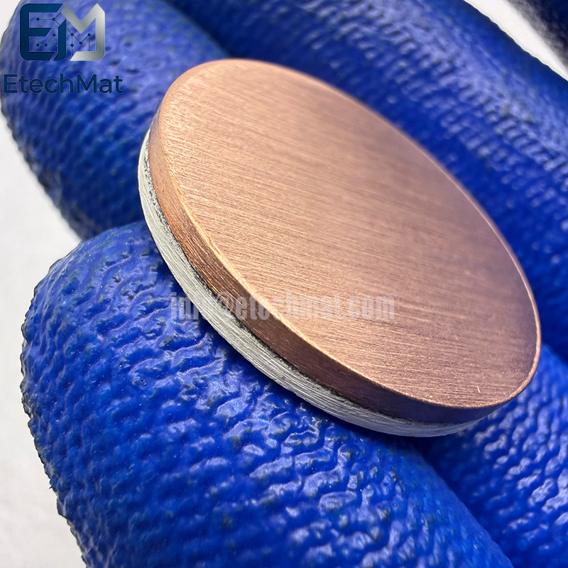
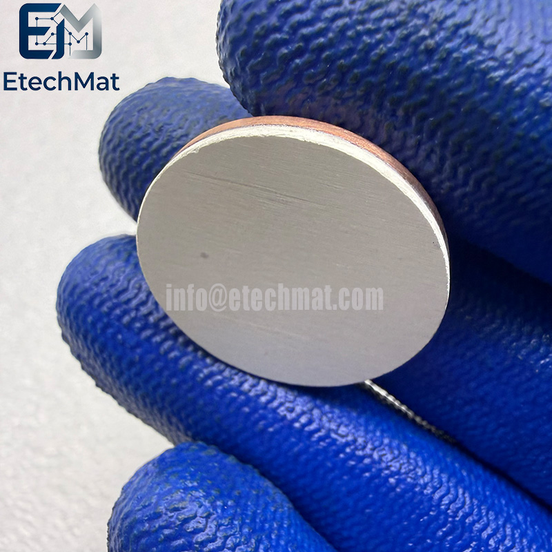
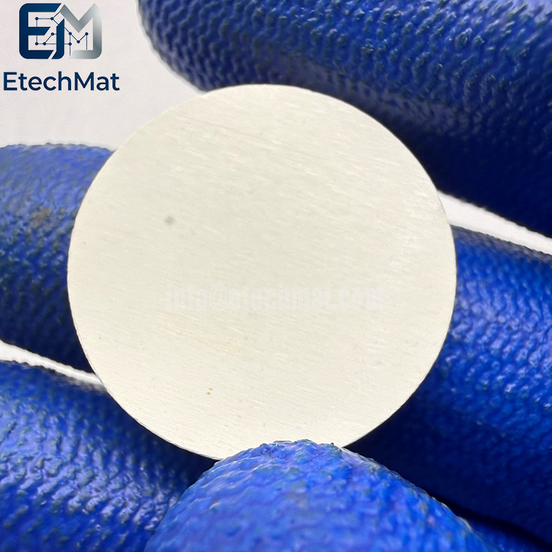
Our ZnS Zinc Sulfide Sputtering Target tackles common challenges in optical thin-film deposition. Many standard ZnS targets suffer from sulfur deficiency and uneven microstructure, which cause inconsistent optical transmission and particle defects that ruin your coated samples. We use high-purity raw materials and carefully controlled sintering processes to preserve the precise ZnS stoichiometry. The dense, homogeneous bulk limits sulfur escape during sputtering and minimizes particulate generation, making this target well suited for infrared coatings, optical windows, and lab optoelectronic device research. Every target is inspected for composition and microstructure before shipment. We supply standard sizes and offer backing plate bonding for stable operation inside your sputtering chamber. Custom shapes and dimensions can also be produced to match your equipment. Cut down wasted substrates from poor film uniformity, so you can focus on collecting reliable optical test data for your projects.
Performance Characteristics of ZnS Zinc Sulfide Sputtering Target
Outstanding optical performance: high refractive index (about 2.35) and wide bandgap (about 3.68 eV), maintaining high transmittance in the ultraviolet to infrared band (8-12 μ m), making it an ideal material for infrared windows and laser optical components.
Good electrical and thermal stability: high electron mobility (>100 cm ²/V · s) and high temperature resistance (>1000 ° C), suitable for extreme environments such as semiconductor devices and aerospace sensors.
Strong chemical stability: corrosion resistance, oxidation resistance, and also has potential applications in the fields of chemical and biomedical engineering.
Applications of ZnS Zinc Sulfide Sputtering Target
Infrared optical coating: used for infrared thermal imager windows and dual-band anti-reflective films (3-5 μ m and 8-12 μ m), with an average transmittance of over 95%.
Solar cell buffer layer: ZnS thin film can be used as a non-toxic alternative material for CdS buffer layer in CIGS solar cells, with better lattice matching with the absorption layer and a wider bandgap.
Optoelectronic devices: used for the preparation of photodetectors, LEDs, and laser diodes, particularly outstanding in ultraviolet detection and blue/ultraviolet LEDs.
Display technology: ZnS-based transparent conductive film is a key material for improving device performance in flat panel displays and touch screens.
Specifications of ZnS Zinc Sulfide Sputtering Target
Circular Sputtering Targets(Diameter): 1.0”2.0”3.0”4.0”5.0”6.0” up to 21”
Rectangular Sputtering Targets(Width x Length): 5” x 12”5” x 15”5” x 20”5” x 22”6” x 20”
Thickness: 0.125”, 0.25”
Shape: Disc/Rectangular
Bonding: Unbonding/Bonding
Purity: 4N(99.99%).
Key points on preparing and using zinc sulfide sputtering targets
Target manufacturing:
Common methods include hot pressing, sintering, and spark plasma sintering (SPS). SPS can produce highly dense targets with a relative density above 99%, and it significantly shortens production time.
Key magnetron sputtering parameters:
- Power: Affects crystallinity, thickness uniformity, and optical/electrical properties of the film. Too high a power can overheat the target and reduce film quality.
- Working pressure: Argon is typically used. Pressure should be optimised to control plasma density and energy distribution.
- Substrate temperature: Research shows that at around 350°C, ZnS films can achieve over 80% transmittance in the visible range, with a bandgap of about 3.79 eV.
- Target selection: Choosing a high‑purity target with good crystallinity and uniform physical form is essential. This directly affects sputtering stability and film quality.


