




Previous
Next
IGZO1:1:1 ratio 99.99% Pure Sputtering Target
Description of IGZO1:1:1 ratio 99.99% Pure Sputtering Target
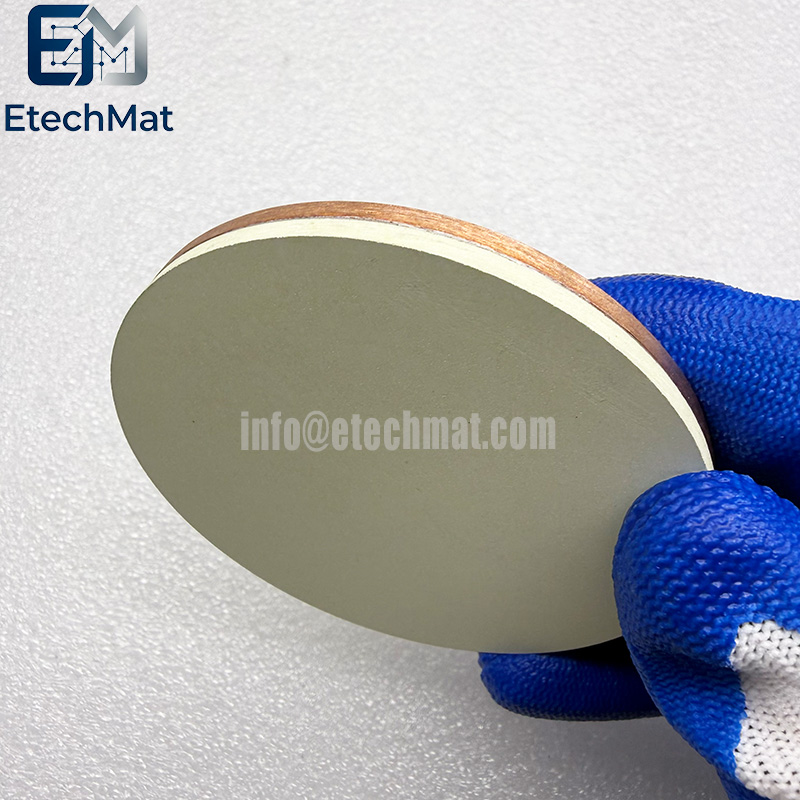
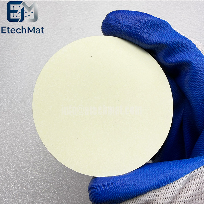
IGZO targets with strict 1:1:1 stoichiometry serve as core sources for oxide‑semiconductor thin‑film transistor fabrication. Minor stoichiometry shift or impurity inclusion during manufacturing can alter carrier mobility, bringing inconsistent electrical performance across deposited layers and undermining R‑D test repeatability. Our IGZO 1:1:1 ratio 99.99% pure sputtering target is produced from high‑purity raw powders with precise compounding and controlled sintering cycles. It maintains a well‑distributed phase structure over the whole target body, delivering homogeneous semiconductor films for TFT research, flexible‑device prototyping and optoelectronic component development. Every target undergoes stoichiometry verification, impurity testing and careful surface examination before shipment. Optimized for RF sputtering in R‑D laboratories and pilot production lines. Its stable material properties reduce performance deviation, helping you get dependable and comparable test data for your advanced optoelectronic thin‑film projects.
Material and Composition
Composition: A composite oxide ceramic target material made by mixing and sintering indium oxide (In ₂ O3), gallium oxide (Ga ₂ O3), and zinc oxide (ZnO) in a specific ratio.
The atomic ratio of 1:1:1 is an ideal ratio for preparing semiconductor thin film transistors, with high electron mobility and switching current ratio. It is the most common and classic formula in IGZO target materials.
Purity level: 99.99% (4N); purity means extremely low metal impurity content, which can effectively avoid defects introduced by impurities during the thin film deposition process and ensure the stability of device performance.
Features of IGZO1:1:1 ratio 99.99% Pure Sputtering Target
1. IGZO 1:1:1 for high-performance displays
2. 99.99% purity for superior thin films
3. Excellent mobility for TFT backplanes
4. Uniform composition for consistent sputtering
5. Ideal for OLED and LCD panels
6. Custom sizes for R&D and production
7. Low impurity for device-grade quality
8. Dense target for stable deposition
9. Supplied with purity analysis certificate
10. Vacuum-sealed for immediate use
Working Principle and Applications of IGZO1:1:1 ratio 99.99% Pure Sputtering Target
Sputtering Process: Primarily utilized in magnetron sputtering (PVD), this process involves ion bombardment of a target surface within a high-vacuum environment, causing IGZO atoms to deposit onto a substrate and form an amorphous IGZO (a-IGZO) thin film.
Core Applications: Serving as the channel layer material, this film is critical for manufacturing high-performance thin-film transistors (TFTs); it is widely used in advanced display panels—such as TFT-LCDs and AMOLED/OLEDs—as well as in the field of semiconductor integrated circuits.
Emerging Frontiers: The material is also garnering attention in cutting-edge areas like in-memory computing and flexible displays. IGZO transistors feature ultra-low off-state currents, making them suitable for low-refresh-rate eDRAM designs; furthermore, amorphous IGZO is considered a potential technological alternative to traditional 1T1C DRAM.


