



Previous
Next
HfO2 Hafnium Oxide Sputter Target
Description of HfO2 Hafnium Oxide Sputter Target
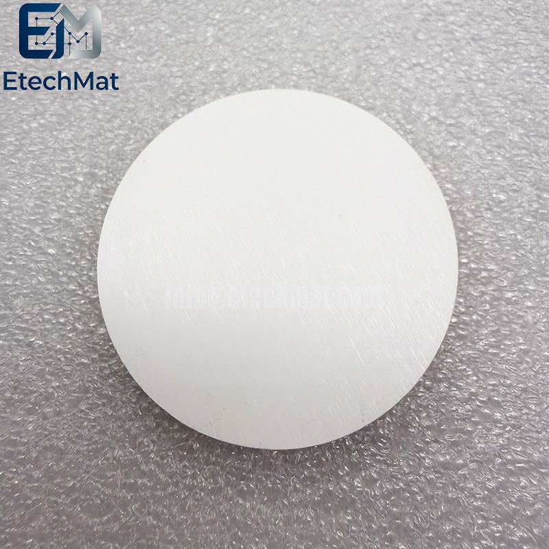
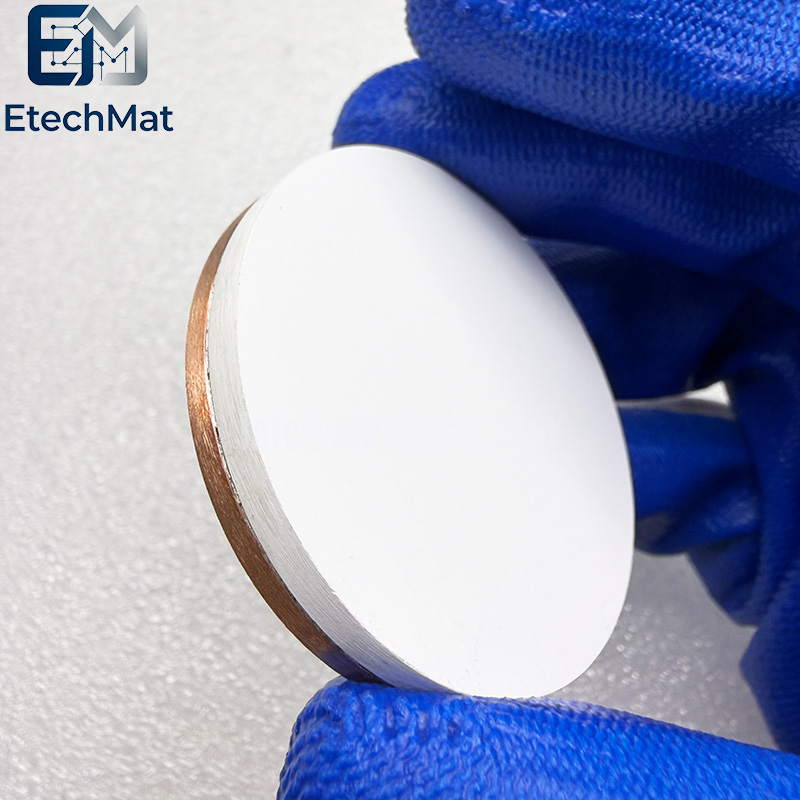
Hafnium oxide serves as a key dielectric material for modern thin‑film technologies, valued for its high‑k properties and excellent chemical stability. Ceramic oxide targets are prone to density fluctuations; internal voids often cause random arcing during RF sputtering, bringing pinholes and uneven dielectric performance to finished thin‑films. Our hafnium oxide sputter target is sintered under careful process control to achieve a consistent bulk density throughout the body. It produces high‑quality dielectric layers fit for semiconductor high‑k gate structures, anti‑reflective optical coatings and academic thin‑film research. Every piece passes density testing, dimensional validation and detailed surface inspection before shipment. It works reliably with lab‑scale RF magnetron systems and pilot deposition equipment. Its stable material performance reduces unplanned arcing incidents, enabling reproducible layer characteristics and advancing your high‑precision electronic and optical device development.
Features of HfO2 Hafnium Oxide Sputter Target
1. High-purity hafnium oxide for thin films
2. Ideal for high‑k gate dielectric layers
3. Dense ceramic for stable deposition rates
4. Excellent optical transparency in the UV range
5. Custom sizes for research and production
6. Low impurity for semiconductor-grade results
7. Suitable for RF and DC magnetron systems
8. Supplied with purity and density certificates
9. Vacuum-sealed for moisture protection
10. Reliable performance for DRAM and logic
Applications of HfO2 Hafnium Oxide Sputter Target
Semiconductor high-k gate dielectrics: With a dielectric constant of approximately 25, these materials are ideal replacements for traditional SiO₂ in the gate insulation layers of CMOS transistors at the 22nm node and below, effectively suppressing leakage current and enabling continued device scaling.
Microelectronic devices: Also used in the development of insulation layers for novel memory and logic devices, such as ReRAM, FeRAM, and ferroelectric tunnel junctions.
Other fields: Can serve as precursors for producing hafnium metal for nuclear control rods, stabilizers for thermal barrier coatings, and scintillators for medical imaging.
Specifications of HfO2 Hafnium Oxide Sputter Target
Circular Sputtering Targets(Diameter): 1.0”2.0”3.0”4.0”5.0”6.0” up to 21”
Rectangular Sputtering Targets(Width x Length): 5” x 12”5” x 15”5” x 20”5” x 22”6” x 20”
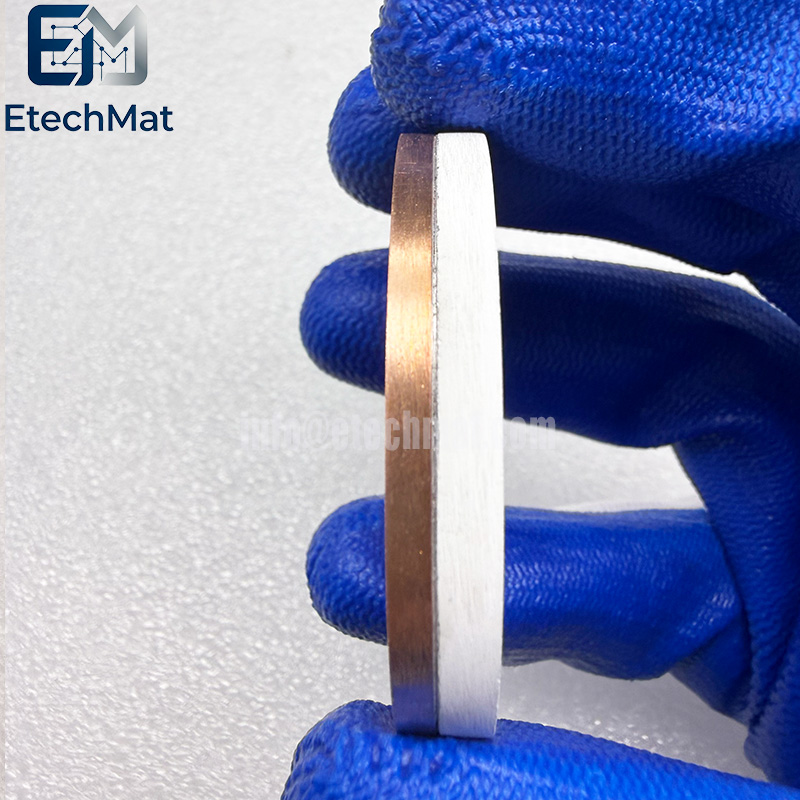
Thickness: 0.125”, 0.25”
Shape: Disc/Rectangular
Bonding: Unbonding/Bonding
Purity: 2N(99%), 3N(99.9%), 3N5(99.95%), 4N(99.99%).


