




Previous
Next
Gallium Oxide 99.95% Pure Sputter Target
Description of Gallium Oxide 99.95% Pure Sputter Target
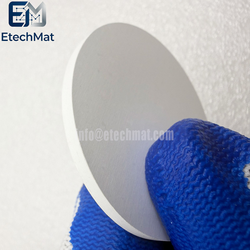
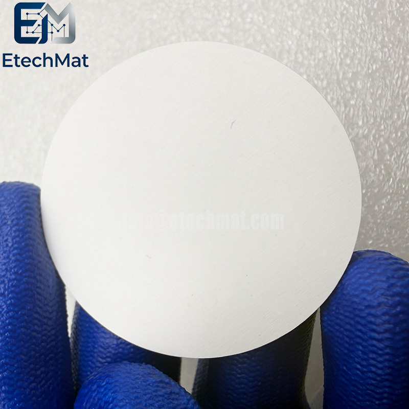
Gallium Oxide 99.95% Pure Sputter Target is designed for thin-film deposition where material consistency, purity, and process control are essential. Made from high-purity gallium oxide, it provides a reliable material source for sputtering processes used in semiconductor research, electronic devices, optical coatings, and other advanced materials applications. For engineers, the real challenge is often not finding a gallium oxide target, but maintaining stable deposition conditions from one production run to the next. This target is manufactured with controlled composition and uniform material quality to support consistent sputtering behavior and predictable film formation. Its stable properties can help reduce process adjustments, unnecessary material loss, and interruptions caused by inconsistent target performance. The 99.95% purity level makes this gallium oxide sputter target a practical choice for research and industrial applications that require controlled material quality without unnecessarily high material costs. Target dimensions and specifications can also be customized to suit different sputtering systems and experimental requirements. From early-stage material development to repeatable thin-film production, it offers a straightforward and dependable solution for customers who value consistency as much as purity.
Features of Gallium Oxide 99.95% Pure Sputter Target
✅ High purity and low impurity levels
✅ Ultra-wide bandgap electrical properties
✅ Dense, stable, and process-compatible characteristics
✅ Versatile environmental resilience
Applications of Gallium Oxide 99.95% Pure Sputter Target
Wide-bandgap power semiconductors: Used to fabricate epitaxial thin films for high-voltage power diodes, MOSFETs, and other devices; significantly reduces power electronic system losses and size; suitable for applications such as ultra-high-voltage power transmission and new energy vehicles.
Solar-blind UV detection: Used to fabricate sensitive thin films for deep-ultraviolet (DUV) photodetectors; enables precise detection of UV signals in the 200–280 nm range without cooling; utilized in fields such as missile early warning and environmental UV monitoring.
Optoelectronic devices: Used to fabricate functional layers for DUV LEDs and UV lasers; fills the performance gap left by traditional semiconductor materials in the DUV wavelength range.
Transparent electronic devices: Used to fabricate high-mobility transparent oxide semiconductor thin films for TFT drive circuits in large-format display panels; enhances panel response speed and resolution.
Cutting-edge research: Widely compatible with magnetron sputtering systems in universities and research institutes; supports research into frontier areas such as novel ultra-wide-bandgap semiconductor materials and quantum devices.
Specifications of Gallium Oxide 99.95% Pure Sputter Target
Circular Sputtering Targets (Diameter): 1.0”, 2.0”, 3.0”, 4.0”, 5.0”, 6.0”, up to 12”
Rectangular Sputtering Targets (Width x Length): 5” x 12”, 5” x 15”, 5” x 20”, 5” x 22”, 6” x 20”
Thickness: 0.125”, 0.25”
Shape: Disc/Rectangular
Bonding: Unbonded/Bonded
Purity: 3N5 (99.95%)


