





Previous
Next
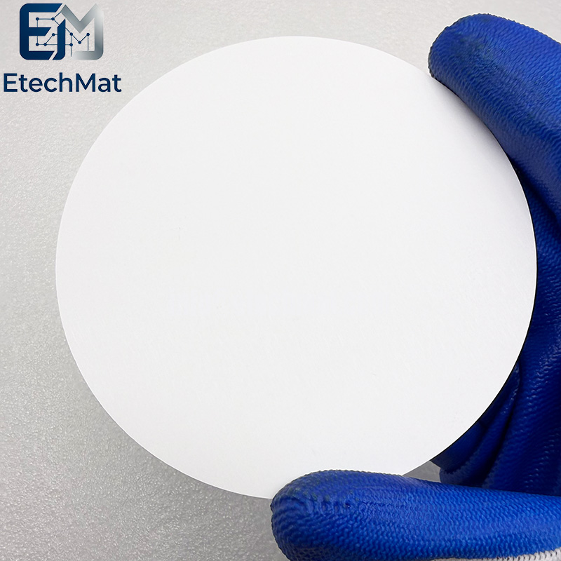
Ga2O3 Gallium Oxide Sputter Target
Description of Ga2O3 Gallium Oxide Sputter Target
Our Ga₂O₃ Gallium Oxide Sputter Target tackles common challenges in wide-bandgap thin-film research. Conventional gallium oxide targets often have uneven density and unstable oxygen content, creating film defects and inconsistent electrical results that disrupt your device experiments. We use carefully selected oxide powder and controlled sintering to build a dense, homogeneous target body. Its stable microstructure maintains reliable stoichiometry during sputtering, lowering oxygen vacancies and particle contamination. It suits power semiconductor, UV photodetector, and optoelectronic coating research. Every target passes composition and surface inspection before shipment. Standard sizes are available, and backing plate bonding can be provided for steady chamber operation. Custom dimensions are also offered to fit your PVD setup. Cut down wasted substrates caused by defective films, and dedicate more lab time to gathering consistent electrical and optoelectronic test data for your development projects.
Features of Ga2O3 Gallium Oxide Sputter Target
99.99% high purity ensures the intrinsic semiconductor properties of the deposited thin film, preventing impurities from interfering with carrier concentration and conductivity type.
A highly dense structure significantly reduces particle splashing during sputtering, ensuring a stable deposition rate and excellent film uniformity.
Controlled fine grain size and low surface roughness enable a uniform, stable flux of sputtered atoms, reducing surface defects in the film.
Predominantly features the β-phase crystal structure—the most stable form at room temperature—ensuring high crystal quality in the sputtered epitaxial film.
Applications of Ga2O3 Gallium Oxide Sputter Target
Power electronic devices: Fabrication of high-voltage, high-efficiency Schottky barrier diodes and field-effect transistors (FETs) for high-voltage, high-power applications such as electric vehicles and photovoltaic inverters.
Solar-blind UV detection: Fabrication of detector films sensitive to solar-blind UV light (wavelengths <280 nm) but unresponsive to visible light, suitable for specialized monitoring tasks like power grid corona detection and forest fire early warning.
High-temperature oxygen sensors: Deposited gallium oxide films can stably detect oxygen concentrations in high-temperature environments (700–1100°C), meeting gas-sensing requirements for extreme operating conditions.
Specialty optical coatings: Used to fabricate deep-UV transparent conductive films, UV filters, dielectric protective layers for solar cells, and other optoelectronic devices.
Specifications of Ga2O3 Gallium Oxide Sputter Target
Circular Sputtering Targets (Diameter): 1.0”, 2.0”, 3.0”, 4.0”, 5.0”, 6.0”, up to 12”
Rectangular Sputtering Targets (Width x Length): 5” x 12”, 5” x 15”, 5” x 20”
Thickness: 0.125”, 0.25”
Shape: Disc/Rectangular
Bonding: Unbonded/Bonded
Purity: 4N(99.99%)


