



Previous
Next
Custom 4N Ga2O3 Sputtering Target
Description of Custom 4N Ga2O3 Sputtering Target
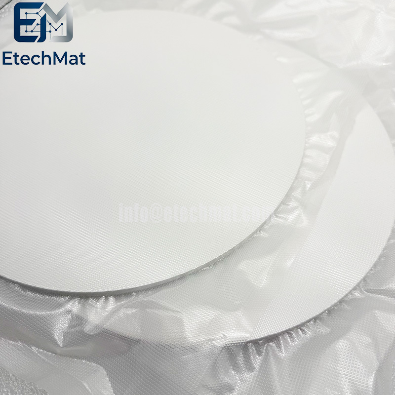
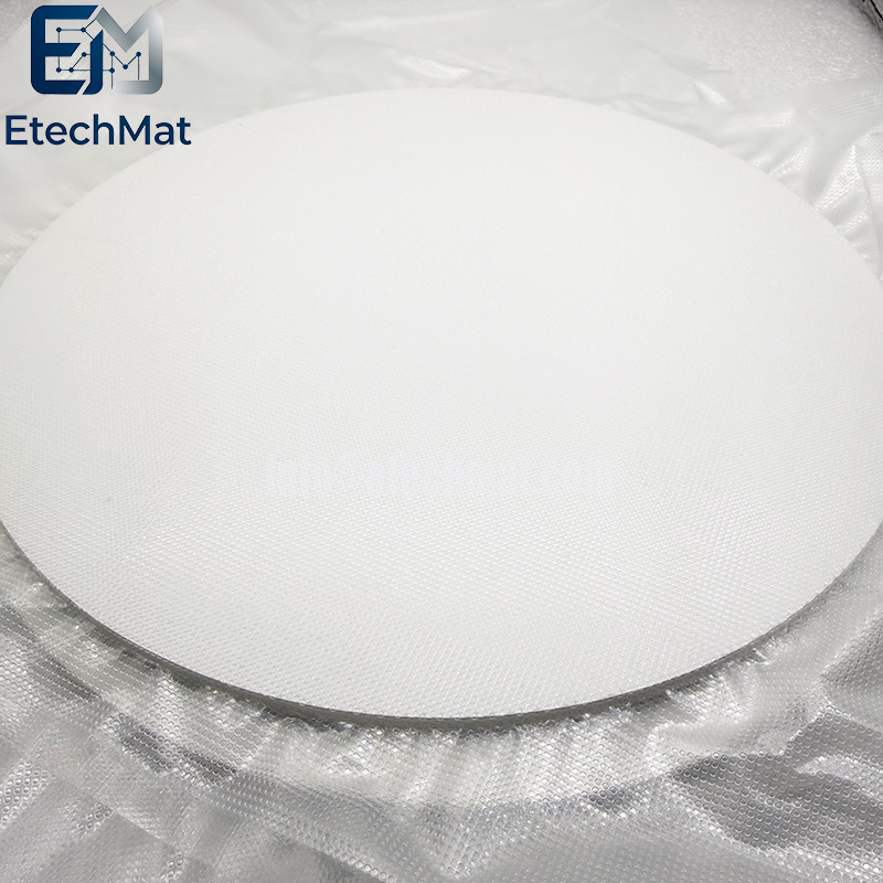
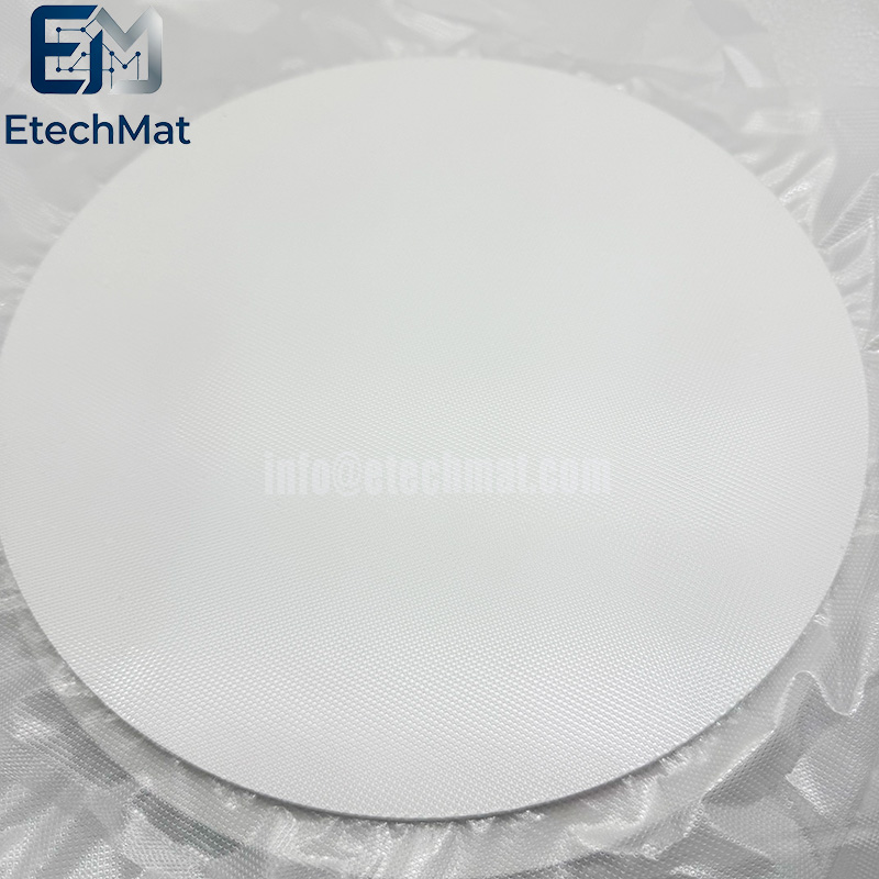
Custom 4N Ga2O3 Sputtering Target is developed for researchers and manufacturers who require high-purity gallium oxide material with precise specifications and reliable sputtering performance. With 99.99% purity, it provides a consistent material source for advanced thin-film deposition, wide-bandgap semiconductor research, power electronics, and optoelectronic applications. In gallium oxide-based device development, material consistency can directly influence film quality, electrical characteristics, and experimental repeatability. This customized sputtering target is produced with controlled composition, uniform material structure, and accurate dimensions to help reduce process variations and improve deposition stability. Unlike standard targets limited to fixed sizes and specifications, the Custom 4N Ga2O3 Sputtering Target is designed around real application requirements. Customers can select suitable dimensions, shapes, and configurations based on different sputtering systems, research goals, and production conditions. This flexibility helps simplify equipment integration and provides better control over thin-film development. With strict quality management throughout manufacturing, the target delivers dependable material performance for demanding applications. Whether used in laboratory research or advanced semiconductor development, it offers a practical solution for customers seeking consistent Ga2O3 quality, stable sputtering behavior, and greater confidence in their deposition process.
Features of Custom 4N Ga2O3 Sputtering Target
High purity: 4N (purity ≥99.99%) with a total impurity content of less than 100 ppm, ensuring high film quality.
Wide-bandgap semiconductor: With a bandgap of approximately 4.8–5.3 eV, it is classified as an ultra-wide-bandgap semiconductor material, making it suitable for high-power and high-frequency device applications.
Key physical parameters: Density of approximately 5.88–6.44 g/cm³ and a melting point of 1740°C; insoluble in water and sparingly soluble in hot acidic or alkaline solutions.
Outstanding electrical properties: Features an ultra-high breakdown field strength (approximately 8 MV/cm), making it suitable for the fabrication of next-generation power semiconductor devices.
Applications of Custom 4N Ga2O3 Sputtering Target
Power Electronics: Used in rectifier modules for EV fast-charging stations, solid-state transformers for smart grids, etc.; gallium oxide thin films feature an ultra-high breakdown electric field strength (approximately 8 MV/cm).
Optoelectronic Devices: Deep-ultraviolet (DUV) LEDs, solar-blind UV detectors, high-energy radiation detectors, etc.
Extreme Environments: High-temperature sensors for aero-engines, neutron flux monitoring in nuclear reactors, and other applications requiring high-temperature and radiation resistance.
Scientific Research: Micro/nano-fabrication, device manufacturing, research on power semiconductor thin films, etc.
Specifications of Custom 4N Ga2O3 Sputtering Target
Circular Sputtering Targets (Diameter): 1.0”, 2.0”, 3.0”, 4.0”, 5.0”, 6.0”, up to 12”
Rectangular Sputtering Targets (Width x Length): 5” x 12”, 5” x 15”, 5” x 20”, 5” x 22”, 6” x 20”
Thickness: 0.125”, 0.25”
Shape: Disc/Rectangular
Bonding: Unbonded/Bonded
Purity: 4N(99.99%)
Manufacturing and Customization Features
Manufacturing Process: Produced using high-purity gallium oxide powder (≥99.95%) via hot-press sintering; compatible with various methods such as cold-press sintering and hot-press sintering.
Customization Flexibility: Diameter, thickness, and copper backing plate bonding are customizable upon request; common specifications include Φ50.8×3 mm and Φ76.2×3 mm, with options for bonding to 2mm or 3mm copper backing plates.
Equipment Compatibility: Suitable for various magnetron sputtering systems, including single-target, multi-target, and ion sputtering setups.
Doping Control: Supports doping with elements such as Sn and Al to tune conductivity type and carrier concentration.


