



Previous
Next
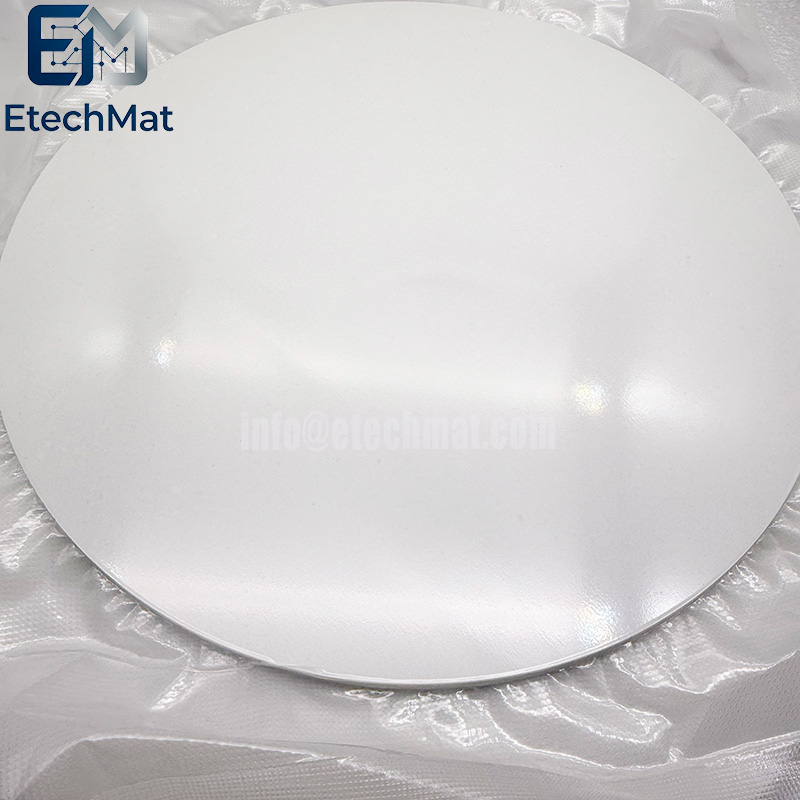
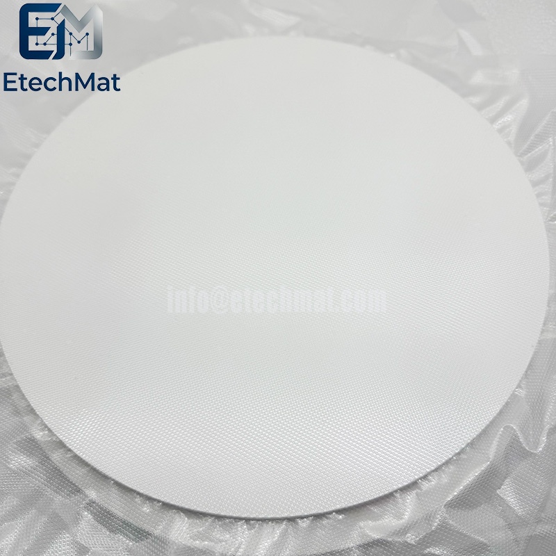
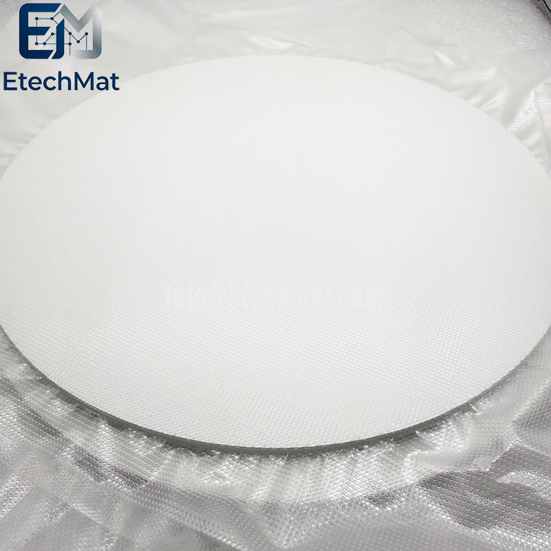
99.99% Pure Ga2O3 Sputtering Target
Description of 99.99% Pure Ga2O3 Sputtering Target
If you're working with Ga₂O₃, you already know how unforgiving it can be. Purity is only part of the story — density, grain size, and bonding quality decide whether your films come out clean or your run ends in a scrapped wafer. Our 99.99% (4N) Ga₂O₃ targets are made with that in mind. We keep impurities low and control the microstructure, so you get stable deposition rates and uniform films run after run. No surprises halfway through a process. We offer custom sizes, thicknesses, and bonding options to fit your existing setup. Whether you're on a lab-scale system or running production, we can match your specs instead of making you work around ours. Every target ships with a certificate of analysis, so you know exactly what you're getting before it goes into the chamber.
Features of 99.99% Pure Ga2O3 Sputtering Target
Purity and Impurities: A purity of 99.99% (4N) implies a total impurity content of less than 100 ppm, effectively preventing impurities from interfering with the electrical and optical properties of the thin films.
Physicochemical Parameters: Chemical formula Ga₂O₃; molecular weight 187.44; melting point approximately 1740°C; appearance as white powder or sintered ceramic targets.
Crystal Structure: Gallium oxide exists in multiple crystalline forms; among them, the monoclinic β-Ga₂O₃ phase is the most stable and the most common in target and thin-film applications. It features an ultra-wide bandgap of approximately 4.9 eV and a high breakdown electric field strength of about 8×10⁶ V/cm.
Applications of 99.99% Pure Ga2O3 Sputtering Target
Power electronic devices: Leveraging high breakdown electric field and high-temperature resistance properties to fabricate high-voltage, high-power devices such as Schottky diodes and field-effect transistors, suitable for new energy vehicles and industrial motor control.
Deep-ultraviolet (DUV) photodetection: Highly sensitive to ultraviolet light in the 200–300 nm range; applicable to flame sensors, environmental monitoring, and aerospace UV detection.
Transparent conductive thin films: Conductivity is tuned via doping (e.g., with tin or silicon) for use in touch screens, smart windows, and flexible display devices.
Scientific research and coating: Widely used in thin-film fabrication for semiconductor chips, solar photovoltaics, flat-panel displays, and specialty coatings; compatible with various magnetron sputtering systems.
Specifications of 99.99% Pure Ga2O3 Sputtering Target
Circular Sputtering Targets (Diameter): 1.0”, 2.0”, 3.0”, 4.0”, 5.0”, 6.0”, up to 12”
Rectangular Sputtering Targets (Width x Length): 5” x 12”, 5” x 15”, 5” x 20”, 5” x 22”, 6” x 20”
Thickness: 0.125”, 0.25”
Shape: Disc/Rectangular
Bonding: Unbonded/Bonded
Purity: 4N(99.99%)
⚠️ Key Considerations
Material Form: 99.99% gallium oxide is commonly sold as a powder; sputtering targets are typically manufactured from high-purity powder through processes such as forming and sintering. When inquiring, clarify whether the product is raw powder or a finished target.
Performance Verification: High purity is merely the baseline; properties such as grain size, density, and crystallographic texture are equally critical. Request analytical reports (e.g., ICP-MS, XRD) upon purchase to verify impurity types and levels.
Customization: Target dimensions, shapes (e.g., rectangular, circular), and bonding methods usually require customization based on the specific sputtering equipment; this affects both manufacturing complexity and cost.


