



Previous
Next
4N Ga2O3-ZnO(Ga2O3 0.5~1wt%) Sputtering Target
Description of 4N Ga2O3-ZnO(Ga2O3 0.5~1wt%) Sputtering Target
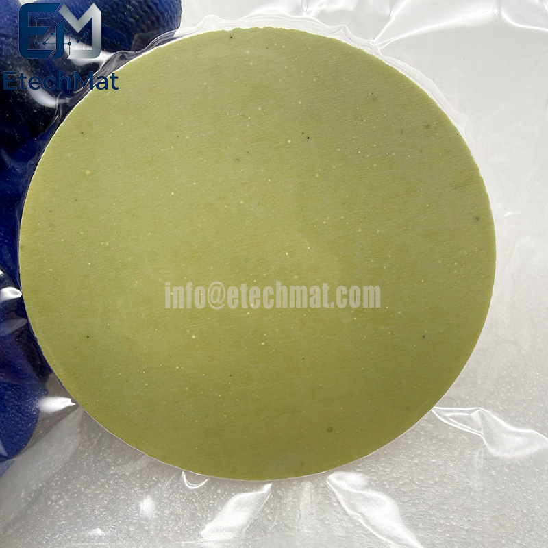
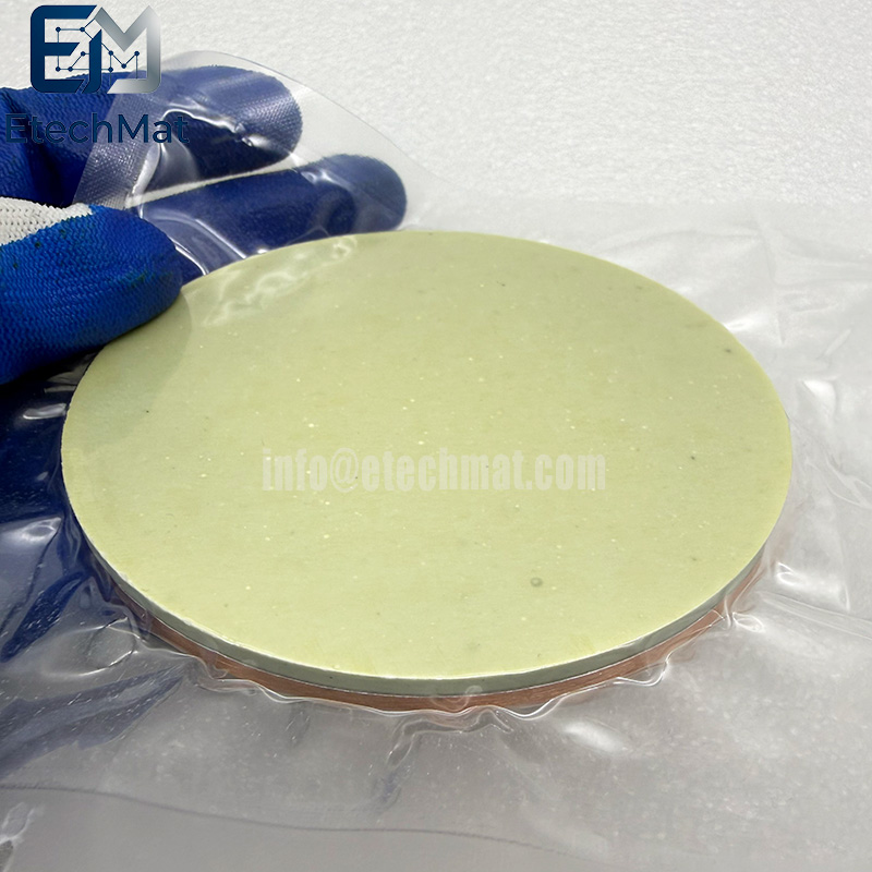
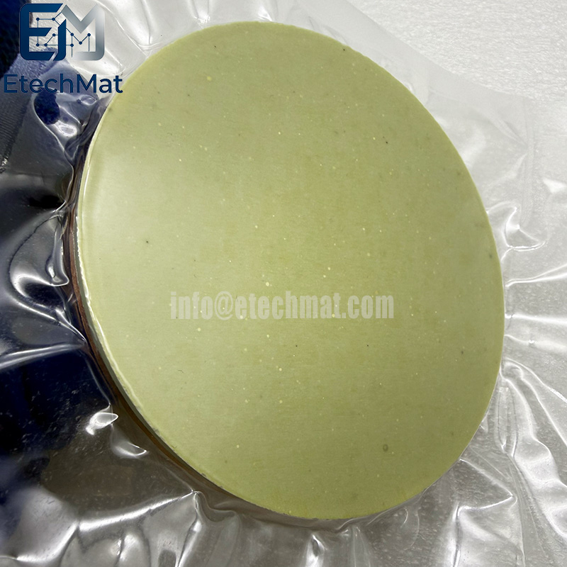
4N Ga2O3-ZnO (Ga2O3 0.5~1wt%) Sputtering Target is designed for customers who need reliable oxide materials with precise composition and stable sputtering performance. With a controlled gallium oxide content of 0.5~1wt% and 99.99% purity, this target provides a dependable material source for transparent conductive films, semiconductor devices, display technologies, and advanced electronic applications. In oxide thin-film deposition, small differences in material composition can influence electrical performance, film uniformity, and overall process stability. This Ga2O3-ZnO sputtering target is manufactured with strict composition control, uniform structure, and consistent quality to help reduce deposition variations and improve repeatable results. Unlike standard targets that focus only on purity values, this material is developed around practical production needs, including stable sputtering behavior, equipment compatibility, and efficient process management. The optimized Ga2O3 addition helps support the development of functional oxide films with controlled properties. Available in customized sizes and specifications, 4N Ga2O3-ZnO (Ga2O3 0.5~1wt%) Sputtering Target can be adapted to different sputtering systems and research requirements. It provides engineers and manufacturers with a dependable solution for developing high-quality transparent conductive and next-generation electronic materials.
Features of 4N Ga2O3-ZnO(Ga2O3 0.5~1wt%) Sputtering Target
1. Doping Mechanism: Gallium atoms substitute for zinc atoms, acting as n-type dopants that provide additional charge carriers to the system, thereby enhancing electrical conductivity.
2. Performance: In heavy doping studies, thin films sputtered from ZnO: Ga₂O₃ (97:3 wt%) targets achieve a resistivity of approximately 2.42×10⁻⁴ Ω·cm, a carrier concentration of about 8.05×10²⁰ cm⁻³, and a Hall mobility of around 32.1 cm²/V·s. Lightly doped films (0.5–1 wt%) exhibit slightly higher resistivity but superior optical transmittance.
3. Conductive Mechanism: Hall mobility in the films is primarily limited by grain-boundary barrier scattering; the barrier height decreases as carrier concentration increases. Additionally, the rise in carrier concentration induces a Burstein-Moss blue shift in the optical bandgap.
4. High Transmittance: ZnO-based films typically achieve an average transmittance exceeding 90% in the visible light range, maintaining high optical transparency even after gallium doping.
5. Bandgap Tuning: Pure ZnO has a bandgap of approximately 3.37 eV; gallium doping allows the optical bandgap to be tuned between 3.18 eV and 3.37 eV, a variation associated with the metal-semiconductor transition.
6. UV Response: Compared to ITO, the GZO system offers advantages in UV transmittance, making it suitable for UV optoelectronic device applications.
Applications of 4N Ga2O3-ZnO(Ga2O3 0.5~1wt%) Sputtering Target
1. Transparent conductive electrodes: Used as an alternative to ITO for transparent electrode layers in flat-panel displays and solar cells.
2. Photodetectors and UV devices: Utilized in ultraviolet optoelectronic components due to its wide bandgap and high transparency.
3. Thin-film transistors (TFTs): Similar to the IGZO system, GZO can be used as the channel layer material in display panels.
Specifications of 4N Ga2O3-ZnO(Ga2O3 0.5~1wt%) Sputtering Target
Circular Sputtering Targets (Diameter): 1.0”, 2.0”, 3.0”, 4.0”, 5.0”, 6.0”, up to 12”
Rectangular Sputtering Targets (Width x Length): 5” x 12”, 5” x 15”, 5” x 20”, 5” x 22”, 6” x 20”
Thickness: 0.125”, 0.25”
Shape: Disc/Rectangular
Bonding: Unbonded/Bonded
Purity: 3N (99.99%)


