




Previous
Next
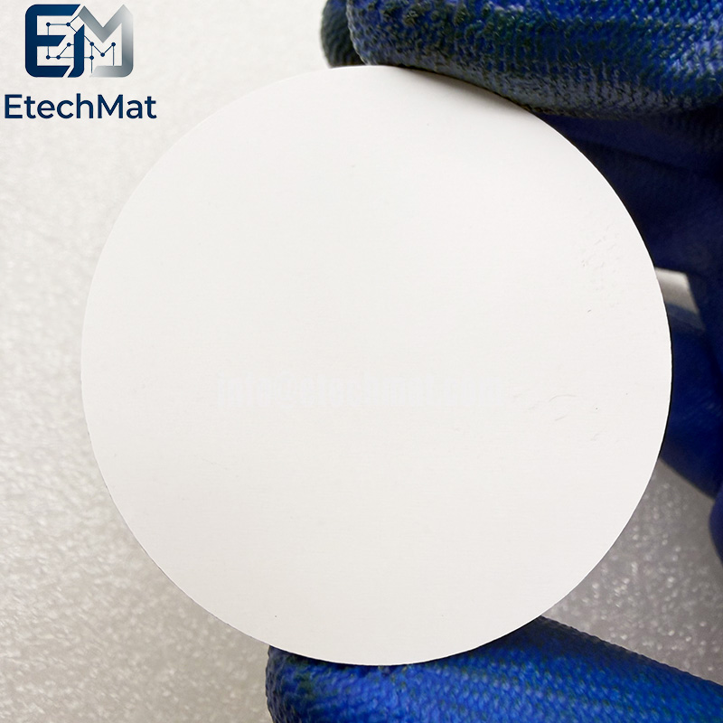
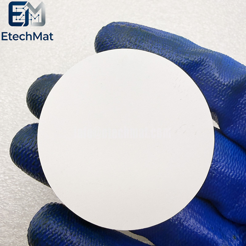
4N Ga2O3 Sputtering Target
Description of 4N Ga2O3 Sputtering Target
Our 4N Ga₂O₃ sputtering target solves common setbacks in wide‑bandgap semiconductor thin‑film preparation. Lower‑quality oxide targets often suffer from uneven phase distribution and oxygen loss, introducing excessive defects that alter band‑gap performance and compromise device‑related experimental repeatability. Using high‑purity raw powders, we adopt refined sintering processes to achieve dense, homogeneous microstructure across the entire target. Tightly controlled fabrication conditions minimise oxygen vacancies and impurity contamination, helping you obtain stable, defect‑moderated gallium‑oxide films for power‑device research, UV‑optoelectronics prototyping and lab‑scale material evaluations. Each target passes strict purity and phase characterisation before dispatch. Standard sizes are readily available, and backing‑plate bonding enables simple chamber mounting. Custom dimensions and shapes can be produced for specialised experimental hardware. Reduce repeated trial‑and‑error caused by defective oxide films, so you can dedicate more lab time to advancing your wide‑bandgap semiconductor research.
Features of 4N Ga2O3 Sputtering Target
1. 4N gallium oxide for advanced electronics
2. High-purity Ga₂O₃ for thin films
3. Excellent wide-bandgap semiconductor properties
4. Ideal for power device applications
5. Dense ceramic for stable sputtering
6. Custom sizes for R&D and production
7. Low impurity for device-grade quality
8. Suitable for RF magnetron sputtering
9. Supplied with purity analysis certificate
10. Vacuum-sealed for contamination protection
Core Features of 4N Ga2O3 Sputtering Target
Electrical performance: High breakdown field strength (up to 8MV/cm), good thermal stability, suitable for high-power devices.
Optical performance: It has good transparency in the deep ultraviolet band and is a key material for solar blind ultraviolet detectors.
Doping control: Supports doping of elements such as Sn and Al, and can adjust the conductivity type and carrier concentration to meet different device requirements.
Applications of 4N Ga2O3 Sputtering Target
Power semiconductor: an efficient and low-loss power device used in fields such as fast charging piles for electric vehicles, smart grids, and 5G communication.
Optoelectronic detection: preparation of sun blind ultraviolet detectors, deep ultraviolet LEDs, high-energy radiation detectors, etc.
Extreme environmental devices: high-temperature sensors for aircraft engines (capable of working for over 1000 hours at 1200 ℃), neutron flux monitoring for nuclear reactors, etc.
Specifications of 4N Ga2O3 Sputtering Target
Circular Sputtering Targets(Diameter): 1.0”2.0”3.0”4.0”5.0”6.0” up to 21”
Rectangular Sputtering Targets(Width x Length): 5” x 12”5” x 15”5” x 20”5” x 22”6” x 20”
Thickness: 0.125”, 0.25”
Shape: Disc/Rectangular
Bonding: Unbonding/Bonding
Purity: 4N(99.99%).


