



Previous
Next
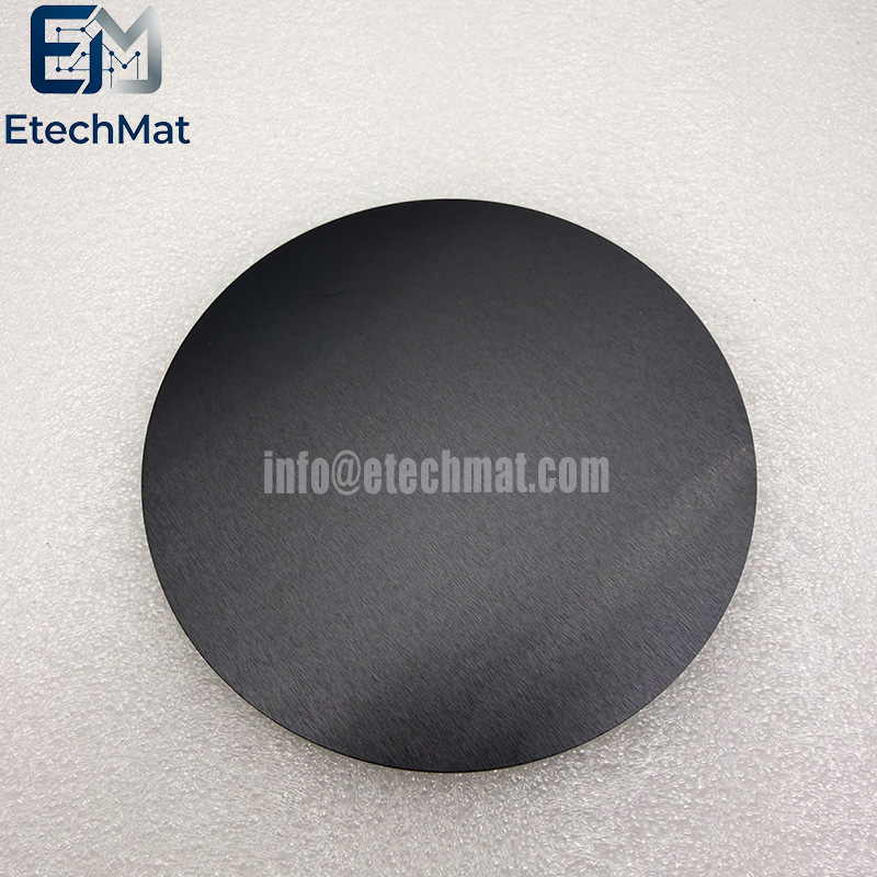
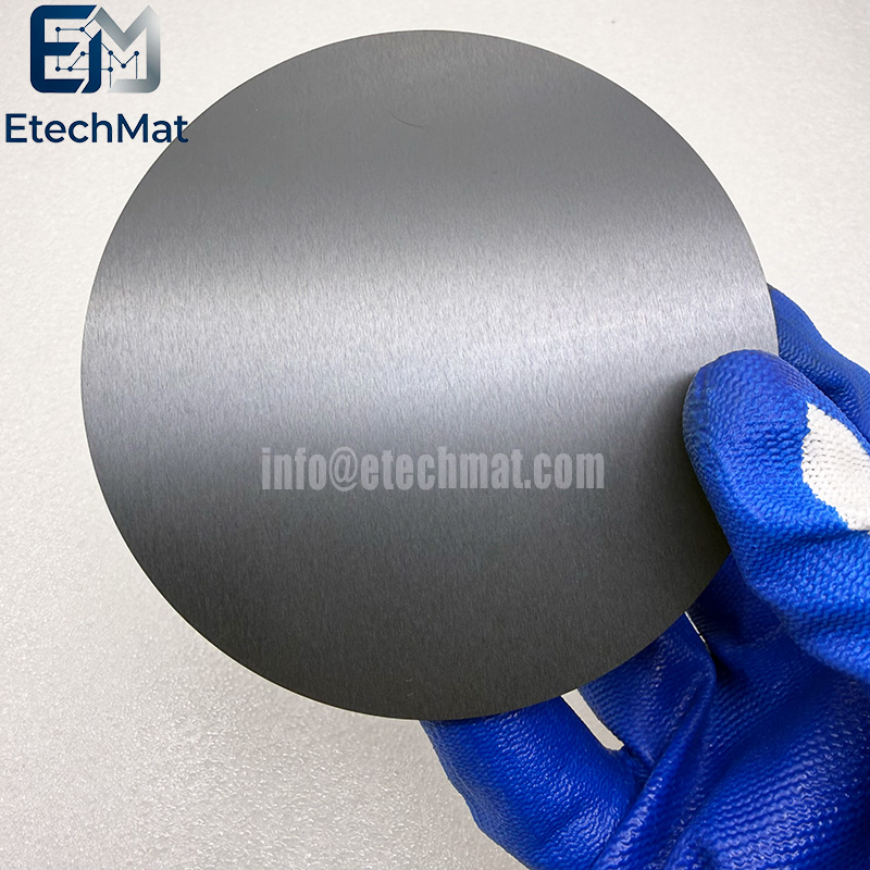
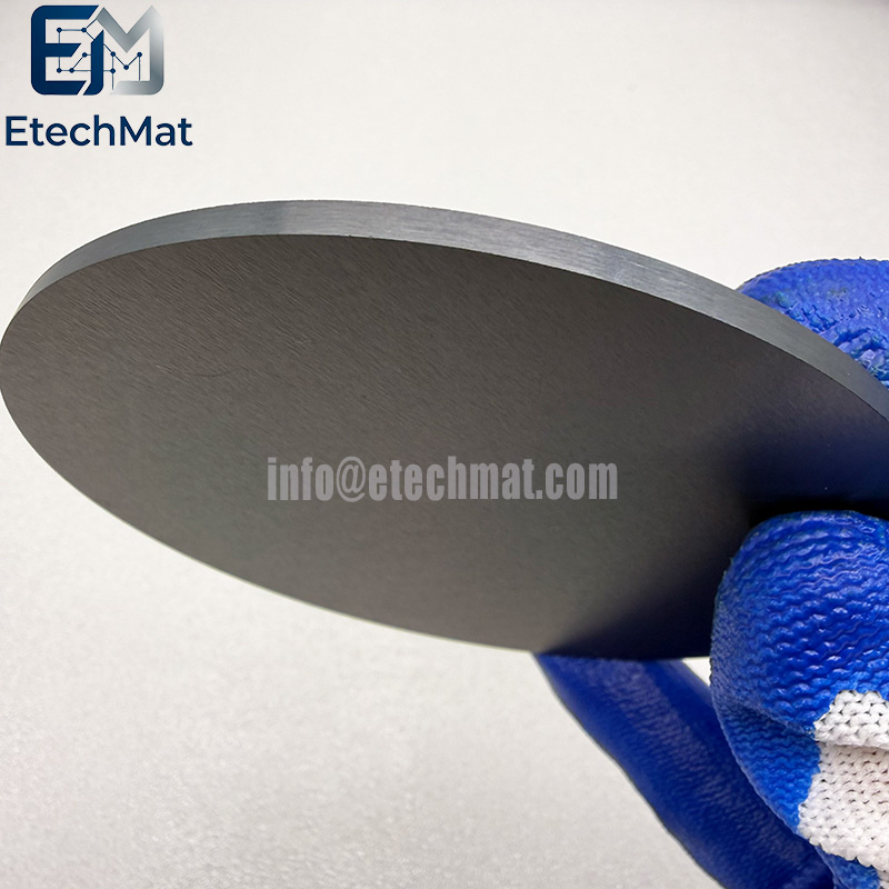
3N Nb2O5 Niobium Oxide Sputtering Target
Description of 3N Nb2O5 Niobium Oxide Sputtering Target
Our 3N Nb₂O₅ Niobium Oxide Sputtering Target addresses common issues in dielectric thin film deposition. Many niobium oxide targets suffer from inconsistent density and uneven grain distribution, leading to particle contamination and fluctuating refractive index, which ruins your optical coating and microelectronic device tests. We use carefully selected raw powder and controlled sintering to create a dense, homogeneous target body. This stable microstructure maintains consistent stoichiometry during sputtering, reducing defects and ensuring uniform dielectric films. It works well for anti-reflection coatings, optical filters, capacitors, and semiconductor research. Each target goes through strict composition and surface inspection before shipment. Standard sizes are available, and backing plate bonding service can be provided for stable operation inside your vacuum chamber. Custom shapes and dimensions are also offered to match your PVD setup. Minimize wasted substrates caused by unstable film performance and get repeatable optical and electrical data for your R&D projects.
Production Process for 3N Nb2O5 Niobium Oxide Sputtering Target
The main route is powder metallurgy. This includes cold isostatic pressing (CIP) followed by high‑temperature sintering. Hot pressing (HP) or hot isostatic pressing (HIP) can also be used to achieve higher density.
Key indicator – relative density:
Commercial targets typically range from 90% to 99%. Density directly affects sputtering performance.
- 90–93%: Lower sputtering rate. The target surface tends to overheat locally, and particle ejection may occur. Suitable for low‑end optical coatings.
- 95–97%: Mainstream level. Stable sputtering with acceptable film uniformity. Suitable for general industrial optics and touch screens.
- ≥98%: High density with few pores. High and stable sputtering rate. Dense films. Suitable for high‑precision optics and semiconductor dielectric layers.
Risks of low density:
Too many pores can cause plasma arcing at the pores during sputtering. Ejected particles landing on the substrate create film defects. In laser optics or semiconductor gate applications, this can ruin an entire wafer.
Features of 3N Nb2O5 Niobium Oxide Sputtering Target
1. Excellent refractive index for multilayers
2. Ideal for interference filters and mirrors
3. Dense ceramic for stable deposition
4. Custom sizes for R&D systems
5. Low impurity for consistent film quality
6. Suitable for RF magnetron sputtering
7. Supplied with composition certificate
8. Vacuum-sealed for contamination protection
Applications of 3N Nb2O5 Niobium Oxide Sputtering Target
Optical Thin Films (Primary Application Area): Used in conjunction with SiO₂ to deposit anti-reflective coatings, high-reflectivity coatings, and optical filters for applications such as camera lenses, laser windows, solar cell cover glass, and optical communication devices. Compared to Ta₂O₅, Nb₂O₅ offers lower costs (due to the higher crustal abundance of niobium), making it a more rational choice.
Semiconductors and Microelectronics: Serves as a high-k dielectric material for gate insulation layers and MIM capacitor dielectric layers; suitable for applications such as power devices, peripheral circuits for memory, and RF MEMS.
Display Panels and Touch Screens: Used as passivation or insulating barrier layers in TFT-LCD and OLED manufacturing processes, leveraging its high density and chemical stability to protect active layers.
Other Applications: Coatings for architectural and automotive glass, gas sensors, optical thin-film interference filters, etc.
Specifications of 3N Nb2O5 Niobium Oxide Sputtering Target
Circular Sputtering Targets (Diameter): 1.0”, 2.0”, 3.0”, 4.0”, 5.0”, 6.0”, up to 12”
Rectangular Sputtering Targets (Width x Length): 5” x 12”, 5” x 15”, 5” x 20”
Thickness: 0.125”, 0.25”
Shape: Disc/Rectangular
Bonding: Unbonded/Bonded
Purity: 3N (99.9%)
⚠️ Selection and Usage Guidelines
Purity Selection: 4N (99.99%) purity is generally sufficient for optical applications; semiconductor gate dielectric applications require 5N (99.999%) or higher, as impurities (especially alkali metals like Na and K, and transition metals like Fe) can introduce interface traps, affecting device threshold voltage and reliability.
Sputtering Method: Nb₂O₅ is an insulating ceramic target; it cannot be powered directly by a DC source and requires RF (Radio Frequency) or MF (Medium Frequency AC) sputtering. If using a magnetron sputtering system, the target must be bonded to a metal backing plate (copper or molybdenum).
Typical Process Parameters: Power density 1–5 W/cm²; working pressure 0.2–1.0 Pa; substrate temperature RT–300°C; target-to-substrate distance 80–150 mm.
Common Issues: Thoroughly clean the chamber before target replacement to prevent target poisoning; excessive film thickness (>500 nm) or low substrate temperatures may lead to cracking or delamination; the refractive index of sputtered films can vary by 0.1–0.2 depending on the equipment and power settings, so optical constants should be recalibrated for precision optical applications.


