



Previous
Next
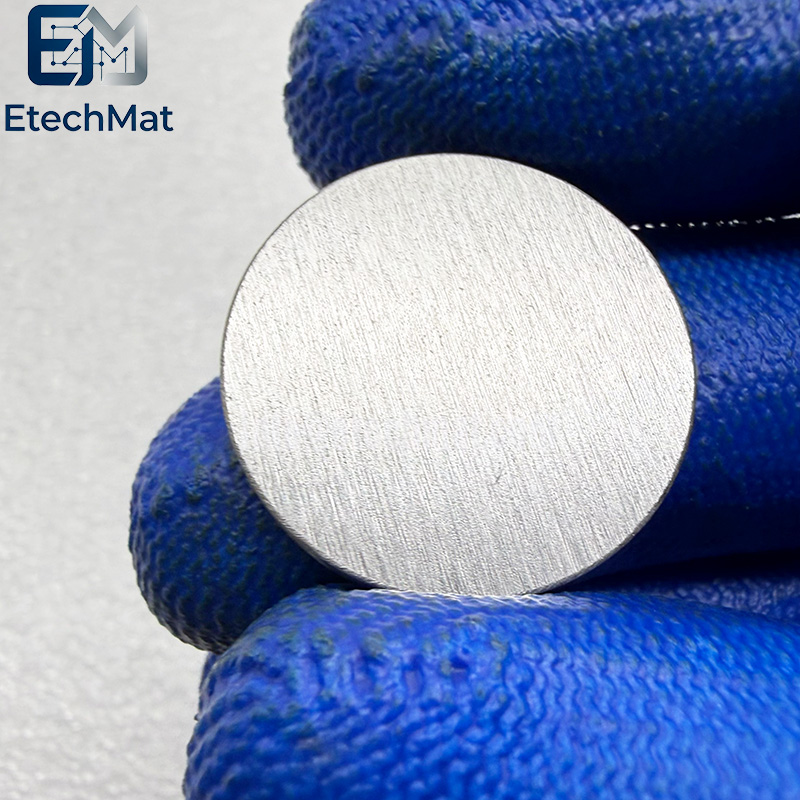
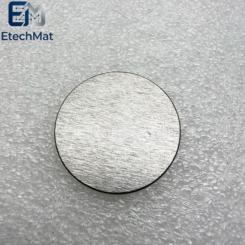
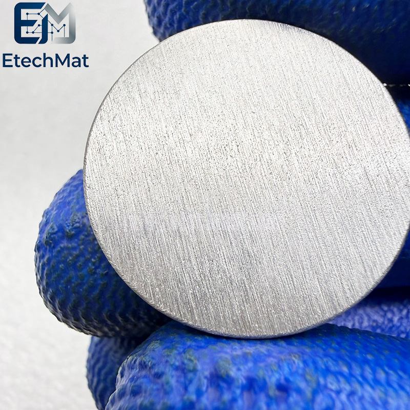
GeSbTe 2/2/5 at% Germanium Antimony Telluride Sputtering Target
Description of GeSbTe 2/2/5 at% Germanium Antimony Telluride Sputtering Target
Our GeSbTe 2/2/5 at% Germanium Antimony Telluride Sputtering Target tackles common challenges in phase-change thin film development. Many standard GST targets suffer from poor elemental homogeneity, leading to compositional variation that alters switching characteristics and produces inconsistent device test results. We blend high-purity raw materials and apply controlled sintering to preserve the required atomic ratio throughout the target. Its dense microstructure minimizes element segregation during sputtering, supporting stable deposition of phase-change layers ideal for PCRAM prototyping and lab performance testing. Every target undergoes composition and uniformity checks before shipment. Standard sizes are available, and backing plate bonding can be provided for steady chamber operation. We also accept custom dimensions to match your PVD setup. Avoid wasted wafers from erratic film properties, and focus your efforts on collecting reliable switching and electrical data for your memory device research.
Features of GeSbTe 2/2/5 at% Germanium Antimony Telluride Sputtering Target
1. GeSbTe 2/2/5 for phase‑change memory
2. High‑purity GST for PCM devices
3. Ideal for non‑volatile data storage
4. Excellent switching speed for memory
5. Custom sizes for R&D systems
6. Dense target for uniform sputtering
7. Low impurity for reliable performance
8. Suitable for RF and DC magnetron
9. Supplied with composition certificate
10. Vacuum‑sealed for contamination control
Applications of GeSbTe 2/2/5 at% Germanium Antimony Telluride Sputtering Target
Phase change memory (PCM): As a prototype material for non-volatile memory, it utilizes the huge resistance difference between crystalline and amorphous states to achieve data storage, with advantages such as high speed, low power consumption, non-volatility, and long data retention time.
Rewritable optical storage: Its phase change characteristics were first used for rewritable optical storage media such as optical discs.
Optical metasurface: Etching nano-grating structures on GST thin films can regulate the reflection, transmission, and absorption of light through phase transition switching, and is used in fields such as dynamic color display.
Thermoelectric materials: The Ge Sb Te system has low electrical resistivity and thermal conductivity, and has great potential for thermoelectric properties.
Specifications of GeSbTe 2/2/5 at% Germanium Antimony Telluride Sputtering Target
Circular Sputtering Targets(Diameter): 1.0”2.0”3.0”4.0”5.0”6.0” up to 21”
Rectangular Sputtering Targets(Width x Length): 5” x 12”5” x 15”5” x 20”5” x 22”6” x 20”
Thickness: 0.125”, 0.25”
Shape: Disc/Rectangular
Bonding: Unbonding/Bonding
Purity: 4N(99.99%).
⚠️ Handling Precautions
Deposition methods: GST films can be deposited by magnetron sputtering (DC or pulsed‑DC), electron‑beam evaporation, or dry‑etched using ICP, RIE, or IBE.
Process effects: Doping (e.g., with Al) or annealing temperature can significantly change the phase‑change temperature and crystal stability of GST. Process parameters must therefore be carefully controlled during preparation.


