




Previous
Next
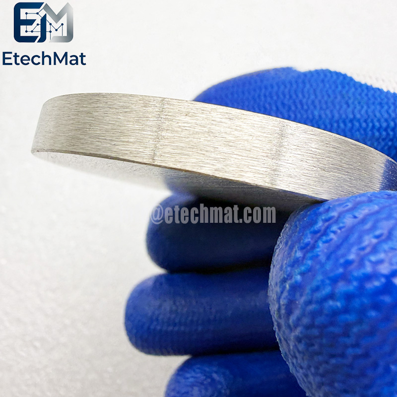
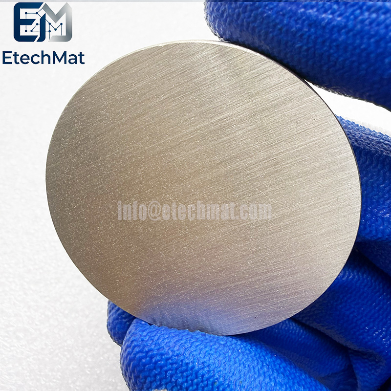
Copper Gallium Alloy Sputtering Target
Description of Copper Gallium Alloy Sputtering Target
Our Copper Gallium Alloy Sputtering Target is made for thin-film deposition processes where alloy composition, material consistency, and equipment compatibility all need to work together. By combining copper and gallium in a controlled alloy system, the target provides a practical material solution for research, process development, and production applications that require a reliable Cu-Ga source. We understand that choosing a sputtering target is not simply about selecting a material from a specification sheet. Target dimensions, shape, bonding method, purity, and composition can all affect how smoothly the material integrates into an existing sputtering system. That is why we can provide customized target configurations based on your equipment and process requirements. Our Copper Gallium Alloy Sputtering Targets can be manufactured in different sizes and geometries, with composition and purity tailored to specific applications where required. Whether you are testing a new deposition process or preparing for repeat production, we focus on keeping specifications clear and consistent from quotation to delivery. Have a specific Cu/Ga ratio, target size, or bonding requirement in mind? Send us your specifications, and we can review the details and help identify a suitable target configuration.
Features of Copper Gallium Alloy Sputtering Target
Composition and Ratios: The gallium content typically ranges from 30% to 68% (atomic percentage), allowing for the formation of intermetallic phases such as CuGa; patented methods also describe the preparation of rotary targets using high-purity (5N or higher) copper, gallium, and indium raw materials.
Material Properties: The CuGa phase is softer than pure CuGa₂, facilitating the production of defect-free targets that exhibit uniform sputtering behavior, thereby enhancing thin-film deposition quality.
Preparation Processes: Common methods include Spark Plasma Sintering (SPS), cold spraying, and medium-frequency induction melting combined with vacuum casting. Vacuum melting processes effectively control impurity levels, compositional uniformity, and gas content while preventing segregation.
Applications of Copper Gallium Alloy Sputtering Target
CIGS Thin-Film Solar Cells: Copper-gallium alloy targets are a key raw material for producing the CIGS (copper-indium-gallium-selenide) light-absorbing layer; the material features high light absorption, making it suitable for thin-film photovoltaic modules.
Semiconductors and Electronic Devices: Sputtering targets are widely used in the deposition of thin films—such as conductive layers and barrier layers—for integrated circuits; copper-gallium alloy targets can be used to deposit functional film layers, including conductive films.
Specifications of Copper Gallium Alloy Sputtering Target
Circular Sputtering Targets (Diameter): 1.0”, 2.0”, 3.0”, 4.0”, 5.0”, 6.0”, up to 12”
Rectangular Sputtering Targets (Width x Length): 5” x 12”, 5” x 15”, 5” x 20”, 5” x 22”, 6” x 20”
Thickness: 0.125”, 0.25”
Shape: Disc/Rectangular
Bonding: Unbonded/Bonded
Purity: 4N(99.99%)


