





Previous
Next
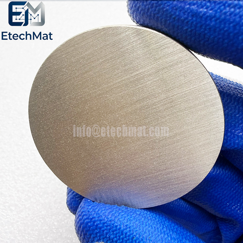
4N Cu70/Ga30 at% Sputtering Target
Description of 4N Cu70/Ga30 at% Sputtering Target
Our 4N Cu70/Ga30 at% Sputtering Target is designed for customers who need a well-defined Cu/Ga composition and dependable material consistency throughout the deposition process. With 99.99% purity and a controlled atomic ratio of 70% copper to 30% gallium, it provides a reliable material basis for thin-film research and production where composition control matters. Rather than treating the target as a standard off-the-shelf component, we can tailor its dimensions, geometry, and bonding configuration to suit your sputtering equipment and process setup. This helps reduce unnecessary adjustments during installation and makes material replacement more straightforward. The target can be supplied for laboratory development, pilot-scale trials, and repeat production requirements. We understand that a sputtering target is only useful when it works with the process around it, so we focus on consistent specifications, clear technical communication, and practical customization. If you have specific target dimensions, bonding requirements, or deposition conditions, share them with us. We can review your requirements and recommend a suitable Cu70/Ga30 target configuration before production.
Features of 4N Cu70/Ga30 at% Sputtering Target
Microstructure: Achieves high density and structural homogeneity, with fine, uniform grains (e.g., average grain size <300 μm), facilitating the production of films with uniform thickness.
Sputtering Performance: Exhibits excellent sputtering characteristics and electrical conductivity, making it suitable for processes such as magnetron sputtering and RF sputtering.
Mechanical Properties: Specific rolling processes yield a high-strength columnar grain structure with controllable ζ-phase orientation, promoting sputtering stability.
Applications of 4N Cu70/Ga30 at% Sputtering Target
CIGS thin film solar cells: This is the core application direction of copper-gallium alloy targets. During the sputtering process, the copper-gallium layer reacts with subsequent elements such as indium and selenium to form a copper indium gallium selenide light-absorbing layer with high photoelectric conversion efficiency.
Semiconductors and Electronic Devices: Copper-gallium alloys can also be used to manufacture high-performance semiconductor devices such as field-effect transistors due to their good electrical and thermal conductivity.
Other functional films: including magnetic recording media, anti-corrosion coatings, anti-reflective coatings, and other vacuum coating fields, as well as the exploration of new processes in materials science research.
Specifications of 4N Cu70/Ga30 at% Sputtering Target
Circular Sputtering Targets (Diameter): 1.0”, 2.0”, 3.0”, 4.0”, 5.0”, 6.0”, up to 12”
Rectangular Sputtering Targets (Width x Length): 5” x 12”, 5” x 15”, 5” x 20”, 5” x 22”, 6” x 20”
Thickness: 0.125”, 0.25”
Shape: Disc/Rectangular
Bonding: Unbonded/Bonded
Purity: 4N(99.99%)
Preparation Method and Process
Raw Materials and Mixing: High-purity copper and gallium metals are selected and mixed in the specified proportions.
Melting and Casting: The mixed materials are melted, refined, and cast into ingots under vacuum conditions.
Rolling and Heat Treatment: The ingot is heated to 700–850°C and held at that temperature for 1–3 hours. It is then rolled over multiple passes (with a reduction of 0.25–1 mm per pass) to form a slab. Finally, the material undergoes leveling, cooling, and machining to produce a target of the required dimensions and shape.


