



Previous
Next
4N GeSbTe 2/2/5 at% GST Sputtering Target
Description of 4N GeSbTe 2/2/5 at% GST Sputtering Target
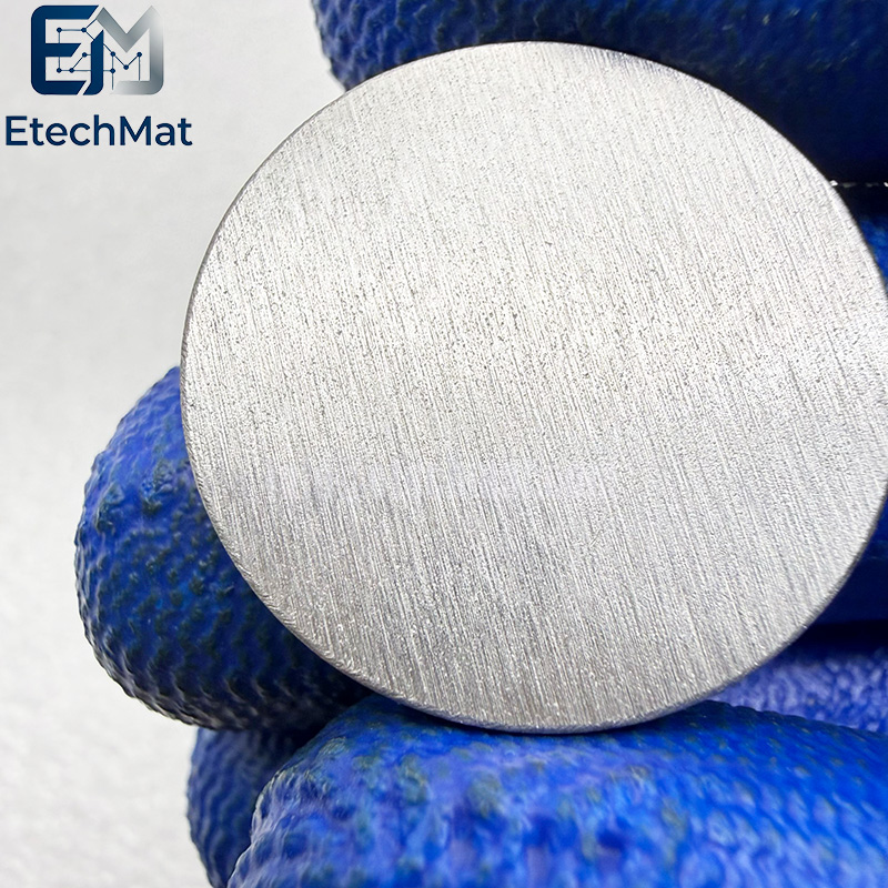
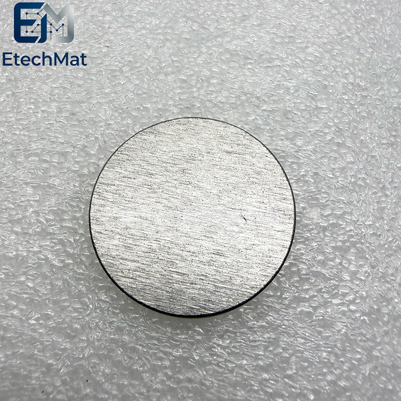
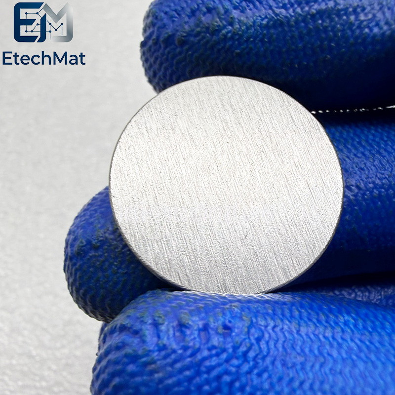
Our 4N GeSbTe 2/2/5 at% GST sputtering target solves typical pain points in phase‑change memory research. Ordinary GST targets often show uneven element distribution and stoichiometry shift during sputtering, which disturbs phase transition behaviour and makes your device test results inconsistent. We adopt high‑purity starting materials and carefully tuned sintering to lock the exact 2:2:5 atomic ratio across the target body. The dense, uniform microstructure reduces element segregation, helping you deposit stable phase‑change films for PCRAM device prototyping and lab evaluation. Each target gets composition and homogeneity checks before delivery. We offer standard dimensions and backing bonding service for steady sputtering runs. Custom sizes can also be manufactured to fit your PVD system. Reduce failed wafer batches caused by unreliable GST films, so you can spend more time gathering consistent electrical and switching performance data for your memory development work.
Features of 4N GeSbTe 2/2/5 at% GST Sputtering Target
1. 4N GST alloy for phase-change memory
2. GeSbTe 2/2/5 for PCM applications
3. High-purity GST for consistent switching
4. Ideal for non-volatile memory devices
5. Custom sizes for R&D systems
6. Excellent crystallization speed for storage
7. Low impurity for reliable device performance
8. Suitable for RF and DC magnetron
9. Supplied with composition analysis certificate
10. Vacuum-sealed for contamination protection
Applications of 4N GeSbTe 2/2/5 at% GST Sputtering Target
Mainly used in the magnetron sputtering process, depositing GeSbTe phase change films, widely used in phase change memory, optical storage media, and integrated storage and computing chips.
Specifications of 4N GeSbTe 2/2/5 at% GST Sputtering Target
Circular Sputtering Targets(Diameter): 1.0”2.0”3.0”4.0”5.0”6.0” up to 21”
Rectangular Sputtering Targets(Width x Length): 5” x 12”5” x 15”5” x 20”5” x 22”6” x 20”
Thickness: 0.125”, 0.25”
Shape: Disc/Rectangular
Bonding: Unbonding/Bonding
Purity: 4N(99.99%).
Preparation and Properties of 4N GeSbTe 2/2/5 at% GST Sputtering Target
Preparation method: GST sputtering targets are typically manufactured using hot pressing sintering to achieve high main‑phase content and high relative density, ensuring uniform film composition during sputtering.
Film properties: GST films deposited at room temperature are amorphous. After annealing at 150–350°C, the films transform from amorphous to a cubic phase, and eventually to a hexagonal phase. This phase‑change behaviour is the basis for data writing and erasing.
Doping modification: Adding elements such as nitrogen, tin, or bismuth can tune GST properties. For example, nitrogen doping increases crystallisation temperature and activation energy, improving amorphous thermal stability. Tin doping may enhance optical storage performance.


