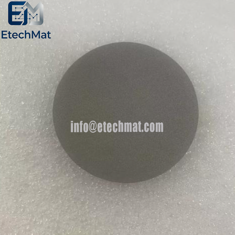
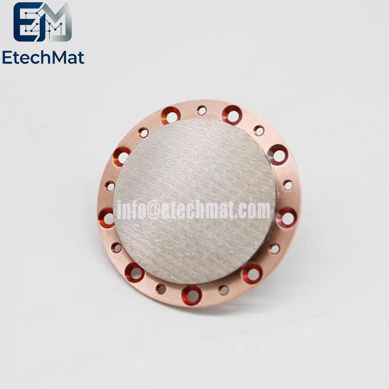
1. Semiconductor Integrated Circuits: This is the application area with the highest technical threshold for sputtering targets. Purity requirements generally exceed 5N (99.999%), while core targets for advanced manufacturing processes below 14nm require 6N (99.9999%) purity—a factor that directly determines chip yield and performance.
Key Target Categories:
Aluminum (Al) and Aluminum Alloy Targets: Used for fabricating metal interconnects and pad layers in chips manufactured via traditional processes.
Copper (Cu) and Copper Alloy Targets: Essential materials for Damascene copper interconnects in advanced processes below 130nm, significantly reducing wiring resistance.
Tantalum (Ta) and Tantalum Alloy Targets: Serve as critical barrier layers in copper interconnect processes, preventing the diffusion of copper atoms into the silicon substrate.
Titanium (Ti) and Titanium-Tungsten (Ti-W) Alloy Targets: Used for contact and adhesion layers to enhance the bonding strength between thin films and the substrate.
Tungsten (W) and Molybdenum (Mo) Targets: Core materials for gate electrodes and word-line layers in 3D NAND flash memory.
Cobalt (Co) and Ruthenium (Ru) Targets: Used for contact layers in advanced logic chips below 7nm, significantly reducing transistor contact resistance.
Hafnium (Hf) Targets: Key raw materials for high-k dielectric thin films in manufacturing processes below 14nm.
2. Flat Panel Display (FPD) Sector: This is currently the largest market for sputtering targets. Over 80% of the world’s display panel production capacity is concentrated in mainland China. Virtually all flat-panel display devices rely on sputtering targets to deposit functional thin films, which directly determine key performance metrics such as screen resolution and light transmission.
Key Sputtering Target Categories:
ITO Targets: Used to produce transparent conductive films; these are the core materials for electrodes in LCD and OLED screens.
Molybdenum (Mo) and Aluminum (Al) Targets: Used for metal wiring layers in panels to establish conductive connections for pixel circuits.
Copper (Cu) and Copper Alloy Targets: Low-resistance wiring materials for large-sized panels (produced on high-generation production lines), helping to reduce screen power consumption.
AZO Targets: A low-cost alternative to ITO for transparent conductive films, widely used in entry-level and mid-range display products.
Silicon (Si) and Silicon Dioxide (SiO₂) Targets: Used to form insulating and passivation layers that protect the panels' internal circuitry.
Tungsten Trioxide (WO₃) Targets: Used as the hole-injection layer in OLEDs, enhancing device luminous efficiency and extending screen lifespan.
3. Solar Photovoltaics (PV): This sector has seen the most rapid growth in demand for sputtering targets in recent years. These targets are primarily used to fabricate functional layers—such as electrodes, barrier layers, and anti-reflective coatings—directly enhancing the photoelectric conversion efficiency of solar cells.
Key Target Categories:
Aluminum (Al) targets: The primary material used for the back electrodes of crystalline silicon (c-Si) solar cells.
Silver (Ag) and silver-alloy targets: Essential materials for the front transparent electrodes of high-efficiency cells, such as TOPCon and HJT cells.
Copper-indium-gallium-selenide (CIGS) alloy targets: The core raw material for the light-absorbing layer in CIGS thin-film solar cells.
Zinc oxide (ZnO) targets: Used to create transparent conductive window layers, which improve the light transmission of thin-film cells.
Silicon dioxide (SiO₂) and aluminum oxide (Al₂O₃) targets: Used to form surface passivation layers on solar cells, reducing the recombination of photogenerated charge carriers.
Molybdenum (Mo) targets: Used as back electrode materials for CIGS cells, facilitating an ohmic contact between the substrate and the light-absorbing layer.
4. Information Storage: This is a traditional core application area for sputtering targets. They are used to fabricate the magnetic thin-film layers of storage media, such as hard disk drives (HDDs) and optical discs; these layers directly determine storage density as well as the stability of data read/write operations.
Key target material categories:
Cobalt-iron (Co-Fe) alloy targets and cobalt-chromium (Co-Cr) alloy targets: Core magnetic thin-film materials for magnetic recording media in hard disk drives.
Chromium (Cr) targets and chromium-vanadium (Cr-V) alloy targets: Used as seed layers for hard disk media to regulate the grain orientation of the magnetic thin films.
Platinum (Pt) targets and palladium (Pd) targets: Core materials for the magnetic tunnel junctions (MTJs) in magnetoresistive random-access memory (MRAM).
Germanium-antimony-tellurium (Ge-Sb-Te) alloy targets: Core phase-change thin-film materials for phase-change memory (PCM), enabling high-speed data reading and writing.
Gadolinium-cobalt (Gd-Co) alloy targets: Materials for the recording layer in magneto-optical discs, enabling rewritable data storage.
5. Other Industrial and Functional Coating Sectors: Encompassing a vast array of downstream applications—such as consumer electronics, mechanical machining, and optical devices—this field utilizes a diverse range of sputtering targets designed to provide specific functional properties, including wear resistance, decorative finishes, and optical performance.
Consumer Electronics and Decorative Coatings: Chromium, titanium, stainless steel, and titanium nitride (ceramic) targets are used to create wear-resistant, decorative coatings for components like smartphone frames and watch exteriors.
Coatings for Hard Cutting Tools and Molds: Tungsten, titanium-aluminum, and titanium carbide (ceramic) targets are employed to produce ultra-hard, wear-resistant surface coatings, extending the service life of cutting tools by 3 to 10 times.
Optical and Optoelectronic Devices: Silicon dioxide, tantalum pentoxide, and magnesium fluoride targets are used to fabricate precision optical thin films, such as anti-reflective coatings for lenses and optical filters.
Electrochromic Applications and Smart Windows: Tungsten trioxide targets are used to create the electrochromic layers in smart dimmable glass, enabling intelligent regulation of sunlight and heat in architectural curtain walls.
Sensors: Platinum, palladium, and tungsten trioxide targets are used to produce the sensitive thin-film layers required for gas, temperature, and humidity sensors.