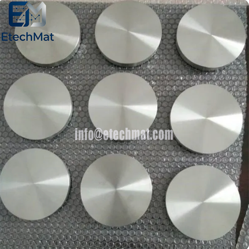
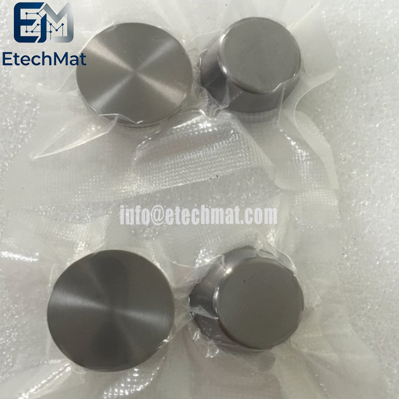
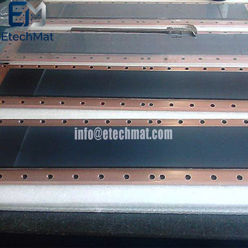
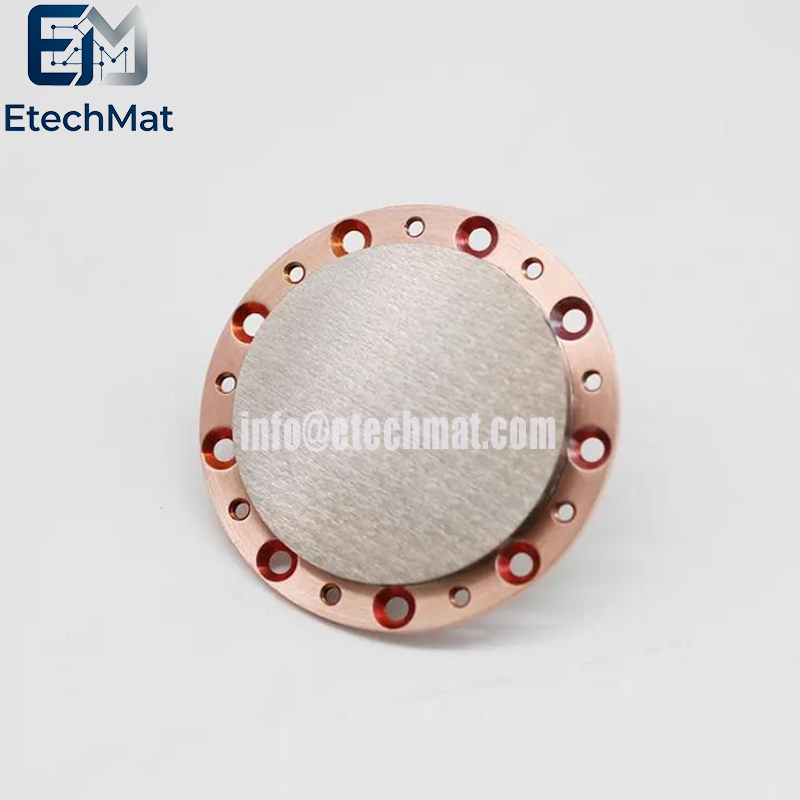
PVD (Physical Vapor Deposition) coating targets are essential consumables in the PVD process. Through physical mechanisms such as magnetron sputtering or vacuum evaporation, solid target materials are converted into atomic-scale particles and deposited onto a substrate surface to form various functional thin films. This technology is widely utilized across the entire high-end manufacturing industrial chain. PVD and CVD (Chemical Vapor Deposition)—the two primary thin-film deposition technologies—differ fundamentally in their underlying principles, process characteristics, and application scenarios.
Key Application Areas for PVD Coating Targets
PVD targets are employed in virtually all high-end manufacturing sectors that require high-precision functional thin films. Performance requirements for these targets vary significantly depending on the specific field:
Semiconductor Integrated Circuits: This represents the application scenario with the highest technical threshold for PVD targets. High-purity (5N grade or higher) materials—such as copper, tantalum, titanium, cobalt, and tungsten—are used to fabricate metal interconnects, barrier layers, and contact layers for chips, supporting thin-film deposition requirements for advanced manufacturing processes at the 7nm node and beyond.
Flat-Panel Displays: Currently the largest market for PVD targets, this sector utilizes materials like ITO (Indium Tin Oxide), molybdenum, aluminum, and copper to create transparent conductive films and metal wiring layers for LCD/OLED panels, ensuring low electrical resistance and high optical transparency.
Solar Photovoltaics: This is the fastest-growing sector in recent years. Targets made of silver, aluminum, molybdenum, or zinc oxide are used to produce transparent electrodes, back electrodes, and passivation layers for high-efficiency HJT/TOPCon solar cells, directly enhancing their photoelectric conversion efficiency.
Precision Optics: Ceramic targets, such as silicon dioxide and tantalum pentoxide, are used to create anti-reflective coatings for lenses and thin-film filters for optical communications, enabling low-loss and high-transmittance performance in optical components.
Energy Storage and Power Batteries: Materials such as copper and nickel are used for base layers in composite current collectors and interface modification layers in solid-state batteries, significantly improving the energy density and cycle life of power batteries. Hard Tool and Decorative Coatings: Sputtering targets made of materials such as titanium, chromium, and titanium-aluminum are used to create ultra-hard, wear-resistant coatings for cutting tools and molds, as well as decorative, protective coatings for 3C electronics, timepieces, and jewelry—serving as an eco-friendly alternative to traditional, highly polluting wet-plating processes.
Superconducting and Quantum Devices: Ultra-high-purity targets, such as niobium and titanium, are used to produce thin films for Josephson junctions in quantum chips and for superconducting detectors. These applications require the concentration of trace magnetic impurities to be controlled down to the parts-per-billion (ppb) level.
Key Differences Between PVD and CVD Coatings
The fundamental distinction between the two lies in their underlying film-formation principles. This core difference leads to significant variations in process conditions, film characteristics, and suitable application scenarios:
Comparison Dimensions | PVD | CVD |
Core Principle | A purely physical process in which a solid target is vaporized—via ion bombardment or heating—and then condenses directly onto the surface of a substrate to form a film; no chemical reactions occur at any stage. | A chemical process in which gaseous precursors are introduced into a reaction chamber, where chemical reactions are initiated via heating or plasma, resulting in the deposition of a solid thin film onto the surface of a substrate. |
Process Temperature | Low-temperature processes, typically carried out in the range of room temperature to 600°C, allow for direct coating onto heat-sensitive substrates such as plastics and aluminum alloys. | High-temperature processes typically operate at 600°C or above, with some reaching up to 1000°C; these are compatible only with heat-resistant substrates. |
Depositable Materials | Covers a vast range of materials, including metals, alloys, ceramics, oxides, and virtually all other solid-state materials. | Only materials that can be formed through reactions involving gaseous precursors can be deposited; these primarily consist of ceramics and insulating dielectric thin films. |
Step Coverage Capability | Line-of-sight deposition offers poor coverage for complex 3D structures with high aspect ratios, and film uniformity is significantly influenced by the shape of the substrate. | Gas-phase molecules can fully penetrate structural gaps, offering excellent step coverage and making them perfectly suited for complex structures such as deep trenches in chips. |
Core Thin-Film Characteristics | The films exhibit extremely high purity, a fast deposition rate, and strong adhesion, making them suitable for the preparation of ultrathin metal/alloy films with a thickness of 10–100 nm. | The thin films exhibit excellent crystallinity and chemical uniformity, along with higher density, making them well-suited for the fabrication of dielectric films with thicknesses ranging from tens to hundreds of nanometers. |
Typical Application Scenarios | Semiconductor metal interconnect layers, display panel electrodes, hard coatings for tools, decorative coatings | Deposition of semiconductor silicon oxide/silicon nitride insulating layers, diamond thin films, and optical fiber preforms. |