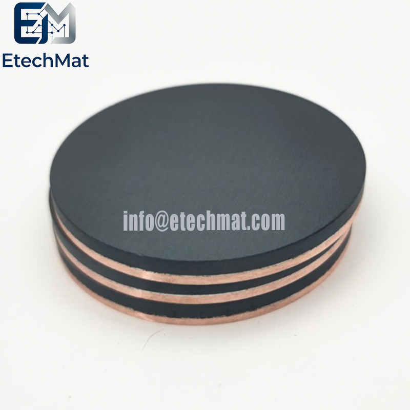
1. What is a Sputtering Target?
A sputtering target is a key consumable material used in physical vapor deposition (PVD) processes. Under a high-vacuum environment, high-energy ions bombard the target surface, causing atoms to be ejected and deposited onto substrates such as wafers and glass to form nanoscale functional thin films.
Simply put, a sputtering target is the material source used in magnetron sputtering, ion beam sputtering, and other PVD coating processes. During the sputtering process, high-energy ions hit the target surface in a vacuum chamber. The atoms from the target are released and then deposited onto substrates such as semiconductor wafers or glass, creating a thin functional film. The target is the material that is consumed during this process.
Notes:
1. A sputtering target is the “material source” for thin film coating.
Structure:
2. Target material (functional layer) + backing plate (support and heat dissipation)
3. Key requirements:
Purity, density, and grain uniformity directly affect thin film quality.
2. Main Classification (By Material)
Metal Targets
Common materials include aluminum, copper, titanium, tantalum, gold, silver, nickel, and chromium.
Alloy Targets
Common materials include aluminum silicon, titanium aluminum, nickel chromium, and other alloy systems.
Ceramic / Compound Targets
Common materials include ITO, AZO, silicon dioxide, titanium dioxide, zinc oxide, and other compounds.
3. Main Application Areas
3.1 Semiconductor Industry (Highest Technical Requirements)
Applications:
Used for wafer interconnect layers, barrier layers, and electrodes, such as copper wiring, titanium/tantalum barrier layers, and titanium adhesion layers.
Key target materials:
High-purity Cu, Ta, Ti, W, and Co.
3.2 Display Panels (Largest Market)
LCD/OLED applications:
ITO targets for transparent conductive electrodes
Mo/Al targets for metal wiring
Metal targets for electrode layers
3.3 Solar Photovoltaics
CIGS thin-film solar cells:
Cu, In, and Ga targets
CdTe solar cells:
CdTe targets
HJT solar cells:
AZO and ITO targets for transparent conductive oxide (TCO) films
3.4 Other Applications
Sputtering targets are also used in:
Optical coatings
Hard coatings for cutting tools
Glass coatings
Decorative coatings (such as titanium and chromium coatings)
Magnetic recording layers for hard disks
4. Key Performance Indicators
Purity
Semiconductor applications: typically ≥5N (99.999%)
Display and photovoltaic applications: typically 3N–4N
Density
Usually ≥98% of theoretical density
Helps reduce pores, impurities, and unstable sputtering performance
Grain Structure
Fine and uniform grains enable more stable and consistent sputtering.
Size
Large-size targets, such as 12-inch semiconductor targets, improve production efficiency and reduce cost per wafer.
5. Basic Requirements for Sputtering Targets
A high-quality sputtering target should have:
High purity
High density
Uniform grain structure
Good electrical and thermal conductivity
Strong bonding with the backing plate
These properties ensure stable sputtering performance and high-quality thin film production.
In addition to industrial coating applications, the term “target material” may also refer to materials used in nuclear physics or X-ray tubes, where the material is bombarded by particle beams or electron beams. However, in the materials and manufacturing industry, “sputtering target” usually refers to the target materials used for thin film deposition.