


Why is it that with the same magnetron sputtering process, others produce uniform, durable coatings while yours scratch at the slightest touch? The answer lies in the sputtering target—think of it as the "paint can" and the sputtering equipment as the "spray gun." If the material in the can is subpar, even the best spray gun won't produce a quality coating! Choosing the wrong target not only results in poor coating performance but can also cause million-dollar equipment to run idly, wasting money.
Step 1: Get to know the "Target Material Family"—choosing the right type saves you from costly missteps!
Different film layers require specific target materials—much like choosing the right flour for a cake; pick the wrong one, and the whole project flops! Here is a quick guide to common types and their applications:
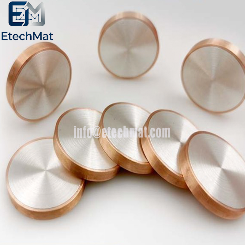
1. Metal Targets: The perfect match for conductive films ⚡
• Key examples: Copper (Cu), Aluminum (Al), and Titanium (Ti) targets
• Applications: Chip interconnects and electrode layers (e.g., the positive current collector in mobile phone batteries)
• Pro-tip: Don't just look at purity for copper targets! Semiconductor-grade requires ≥99.999% (5N) purity; otherwise, impurities cause resistance to skyrocket, turning a 5G chip's performance into "2G speeds." One manufacturer tried to save money using 4N copper targets and saw their defect rate jump from 0.5% to 8%—costing them millions!
2. Ceramic Targets: The heavyweights of insulating and functional films 🛡️
• Key examples: Silicon dioxide (SiO₂), Silicon nitride (Si₃N₄), and ITO (Indium Tin Oxide) targets
• Applications: Wafer insulation layers, anti-blue light screen films, and sensor photosensitive layers
• Fun fact: ITO targets are in the "precious material" league; indium content directly dictates light transmission. At 70% content, transmission is 90%, but drop it to 50%, and it turns into "frosted glass," making your phone screen look instantly murky.
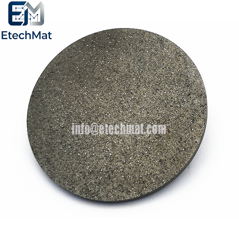
3. Alloy Targets: The "master key" for customized needs 🔑
• Key examples: Aluminum-Silicon (Al-Si) and Titanium-Tungsten (Ti-W) targets
• Applications: Chip contact layers (requiring a balance of conductivity and adhesion)
• Selection tip: Alloy ratios must be precise to two decimal places! For instance, an Al-Si target offers optimal adhesion at 1% silicon; add just 0.5% more, and the material becomes brittle, causing the film layer to crack under stress.
Step 2: Focus on 3 core performance metrics—film quality hinges entirely on them!
Choosing the right type is just the foundation; performance determines the film's "lifespan." You must check these three indicators one by one:
1. Purity: Impurities are the "silent killers" of the film layer ❌
• Industry Golden Rule: Purity must be ≥99.99% (4N) for semiconductor targets, and ≥99.9999% (6N) for high-end chips!
• Real-world Case: A sensor manufacturer used a 3N-grade titanium target for an adhesion layer; oxygen impurities caused the film to delaminate from the substrate. Fingerprint sensor coatings peeled off after just one month, causing user complaints to double.
• Testing Advice: Demand an ICP-MS test report from the supplier. Pay close attention to oxygen, carbon, and iron content—reject anything exceeding 0.001%!
2. Density: A "porous target" means "throwing money down the drain" 💸
• Key Logic: Higher target density leads to more uniform ion sputtering and better material utilization (a 95% density target saves 20% more material than an 85% one).
• Intuitive Check: Weigh it in your hand! For the same volume, a high-density titanium target is 10% heavier than a low-density one—think "solid iron block" vs. "hollow foam." Tests at one factory showed that a silicon nitride target with 98% density improved coating uniformity by 30% and reduced material waste by 15%.
3. Grain Size: The secret behind film "smoothness" 🔍
• Simple Analogy: Target grains are like "sand"—the finer the sand, the smoother the "road surface" (film layer) created.
• Specific Standards: Grain size should be ≤50 microns for semiconductor targets, and ≤10 microns for high-end applications!
• Consequences of Pitfalls: Excessively large grains (>100 microns) cause "bumps" in the film. Mobile phone screens feel noticeably scratchy after coating, and the yield rate is slashed by half.
A final, crucial question to consider 💡: When choosing a target material, should you prioritize the "brand" or the "specifications"?
Industry veterans know the rule: specifications set the baseline, but manufacturing quality determines the upper limit of performance. Even with major imported brands, issues can arise—such as moisture absorption during storage (which can cause ceramic targets to shatter) or impact damage during transit (causing metal targets to deform and leading to uneven sputtering)—resulting in defective products.
My advice to newcomers: First, verify that the specifications meet industry standards. Then, ask the supplier to send samples for trial coating. Relying on actual performance metrics—such as coating adhesion (passing the cross-hatch test without peeling) and uniformity (thickness deviation <2% as measured by a gauge)—is ten times more reliable than listening to sales pitches about "major imported brands."



