




Previous
Next
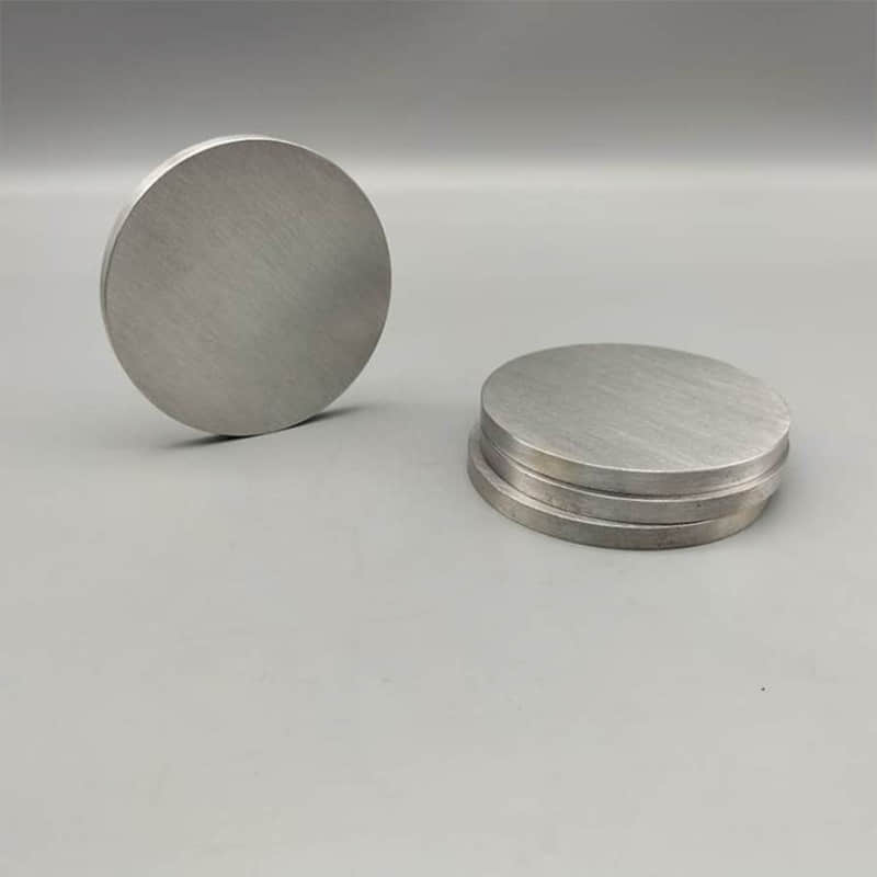
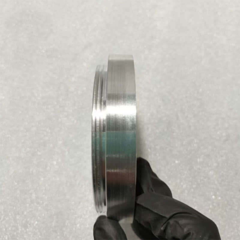
High Purity Magnesium Sputtering Target
Description of High Purity Magnesium Sputtering Target
A high-purity magnesium sputtering target is a critical material used in the physical vapor deposition (PVD) process, specifically in magnetron sputtering systems, to deposit thin films of magnesium onto various substrates. These targets are essential in industries ranging from electronics and optics to automotive and energy storage, where magnesium films offer unique properties such as lightweight, good electrical conductivity, and strong corrosion resistance.
The production of high-purity magnesium targets involves rigorous refinement processes to achieve purity levels typically above 99.9% and often reaching 99.99% or higher. This level of purity is non‑negotiable for thin‑film applications, as even trace impurities can adversely affect film uniformity, adhesion, and overall device performance. State‑of‑the‑art manufacturing techniques, including vacuum melting and hot pressing, are employed to ensure a dense, fine‑grained microstructure with minimal porosity. A well‑consolidated structure is vital to reduce particle spitting and arcing during the sputtering process, which can otherwise compromise coating quality.
In semiconductor fabrication, magnesium‑based films are increasingly explored for use in next‑generation memory devices and barrier layers. In optical coatings, they contribute to the creation of reflective and anti‑reflective layers. Meanwhile, in the battery industry, magnesium thin films are being investigated for their potential in advanced energy storage systems.
With their excellent uniformity, high density, and tightly controlled composition, these targets deliver consistent and reproducible film properties, helping manufacturers achieve superior performance and yield in their deposition processes. In short, a high-purity magnesium sputtering target is not just a consumable—it is an enabler of innovation in modern thin‑film technology.
Core Applications of High Purity Magnesium Sputtering Target
Semiconductors and Next-Generation Memory: Serves as a precursor for the critical insulating barrier layer—specifically the MgO film formed via reactive sputtering—of Magnetic Tunnel Junctions (MTJs) in Magnetoresistive Random-Access Memory (MRAM), thereby determining the device's tunneling magnetoresistance performance; also utilized as a conductive or barrier layer in certain semiconductor devices.
Optical Coatings and Displays: Used to fabricate optical components such as high-reflectivity mirrors, anti-reflective coatings, and optical filters; employed in OLED/LCD applications as specific optical modulation layers or electrode modification layers to enhance brightness and contrast.
Functional Thin Films and Surface Engineering: Used to deposit high-purity magnesium thin films for lightweight alloy coatings, anti-corrosion layers, getter materials, and microelectronic interconnect layers; serves as a reactive target material for producing compound thin films such as magnesium nitride and magnesium fluoride.
Scientific Research and Specialty Applications: Laboratory-scale Physical Vapor Deposition (PVD) research, production of high-purity reducing agents for the nuclear industry, aerospace-grade specialty coatings, and raw materials for fine chemical additives.
Specifications of High Purity Magnesium Sputtering Target
Material Type | Magnesium |
Symbol | Mg |
Atomic Weight | 24.305 |
Atomic Number | 12 |
Color/Appearance | Silvery White, Metallic |
Thermal Conductivity | 160 W/m.K |
Melting Point (°C) | 649 |
Coefficient of Thermal Expansion | 8.2 x 10⁻⁶/K |
Theoretical Density (g/cc) | 1.74 |
Z Ratio | 1.61 |
Sputter | DC |
Max Power Density* | 50 |
Size | 1inch - 8inches/Customized |
Type of Bond | Indium, Elastomer |
Purity | Customized |
Comments | Extremely high rates are possible. |
