


Previous
Next
Custom Nickel Sputtering Target
Description of Custom Nickel Sputtering Target
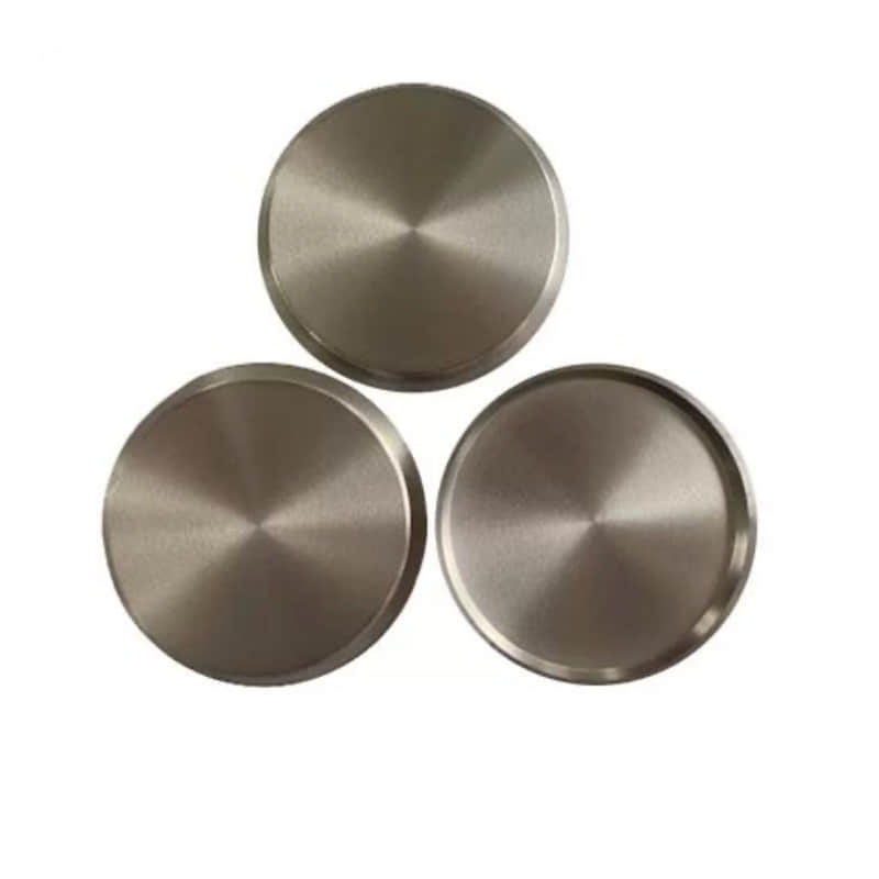
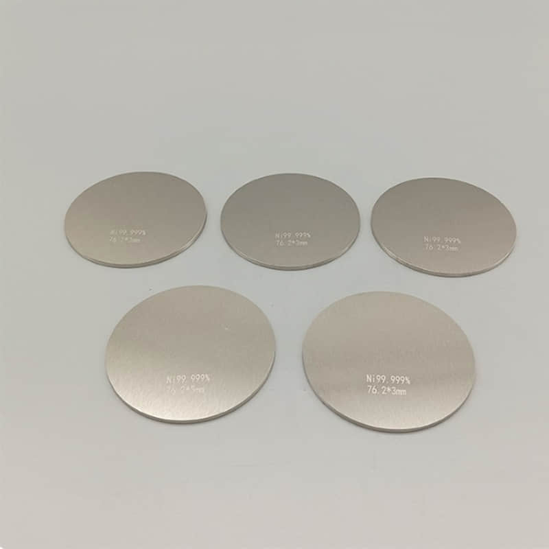
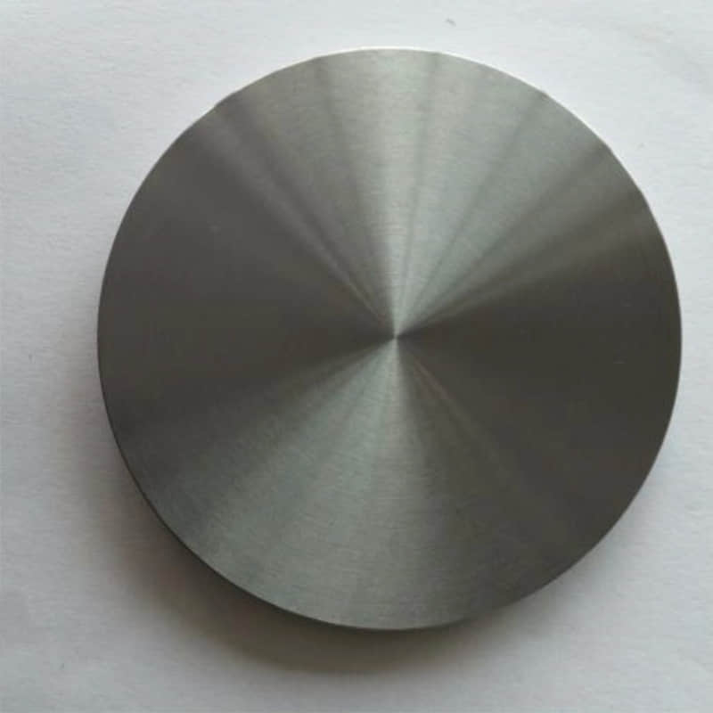
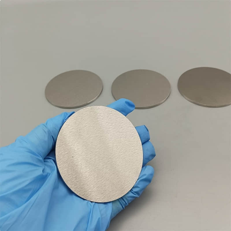
We machine nickel targets to your exact cathode geometry and process requirements. Whether you need a standard disc for a 2-inch source or a complex multi-piece assembly for a large-area coater, we start with vacuum-melted or powder-metallurgy stock and finish to your drawing.
Purity levels range from 3N (99.9%) to 4N5 (99.995%), with full GDMS or ICP-MS certificates showing trace impurities. Grain size and crystallographic texture are controlled through thermomechanical processing, which matters if your film uniformity depends on consistent erosion behavior.
Nickel targets from us have gone into magnetic thin films, diffusion barriers, and underlayers for data storage and semiconductor applications. If your recipe calls for a specific alloy addition—say Ni-Cr, Ni-Fe, or Ni-V—we cast and process those in-house too. Every target is ultrasonically tested for bond integrity if bonded, and vacuum-sealed with desiccant. We keep the paper trail clean: lot numbers, heat numbers, and analytical data all traceable to the original melt.
Applications of Custom Nickel Sputtering Target
Customized nickel sputtering targets are primarily used for semiconductor interconnects and barrier layers, functional films for magnetic storage (MRAM), precision thin-film resistors, electromagnetic shielding coatings, and optical functional films. They are tailored to specific PVD process requirements by adjusting purity (4N–6N), grain size, alloy composition (e.g., NiCr, NiFe, NiW), and geometry.
Semiconductors and Advanced Packaging: Serve as conductive layers, adhesion layers, or diffusion barriers (such as Ni barriers prior to Cu interconnects) to prevent metal migration and extend electromigration lifespan; high-purity nickel (≥4N5) is utilized in advanced wafer fabrication and packaging interconnects.
Magnetoelectronics and Storage Devices: Leverage nickel's soft magnetic properties to fabricate magnetic tunnel junction (MTJ) free/pinned layers and synthetic antiferromagnetic (SAF) layers for MRAM, magnetic sensors, and high-frequency inductors, requiring precise control over coercivity and magnetic permeability.
Precision Electronic Components: Used to fabricate thin-film resistors (often alloyed with Cr to adjust resistance and the temperature coefficient of resistance, or TCR) for hybrid integrated circuits, strain gauges, and high-precision sensors, demanding exceptional compositional uniformity.
Electromagnetic Interference (EMI) Shielding: High-permeability nickel films are deposited on aerospace avionics, 5G/6G modules, and precision instrument housings to provide broadband electromagnetic shielding and wave-absorbing capabilities, thereby suppressing signal interference.
Optical and Decorative Coatings: Serve as reflective layers, neutral density filters, or wear-resistant decorative layers for optical lenses, laser storage media, and surface modification of high-end consumer goods, requiring control over film stress and color consistency.
Specifications of Custom Nickel Sputtering Target
Purity Grades: Standard 3N–4N (99.9%–99.99%); high-end semiconductor applications can reach 5N–6N (99.999%–99.9999%); total impurity content controlled at the ppm level.
Shapes/Types: Planar targets (rectangular/circular), rotary targets (cylindrical), columnar targets, and custom shapes (e.g., dog-bone); supports modular splicing designs.
Dimensions: Planar targets—width 200–1500 mm, thickness 10–50 mm, length up to 4000 mm; rotary targets—outer diameter 50–400 mm, length 3000–4500 mm; specific dimensions customized entirely according to sputtering chamber drawings.
Composition Options: Pure nickel (Ni) or alloys (e.g., Ni-Cr, Ni-Fe, Ni-Co); alloy ratios can be precisely formulated by atomic percentage (at%) or weight percentage (wt%).
Physical Properties: Density typically ≥99.3%; uniform grain size (micron-scale); flatness ≤0.1–0.2 mm/m; some applications require integration with copper backing plates and water-cooling structures.
