




Previous
Next
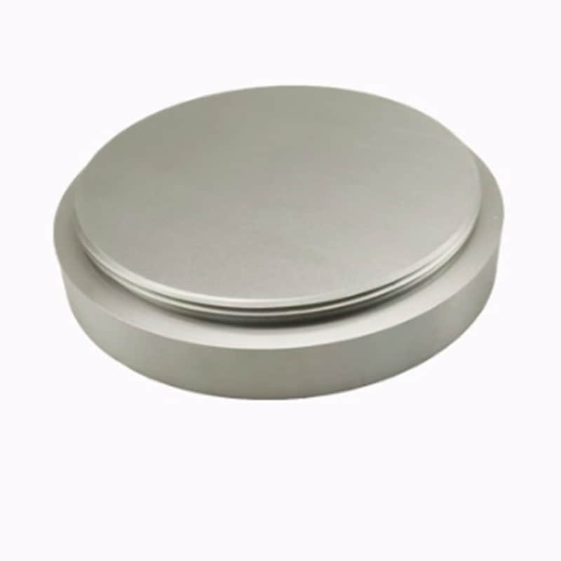
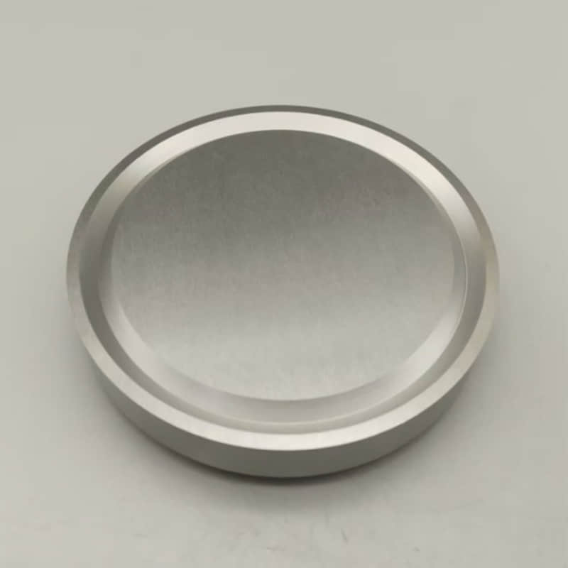
High Purity Molybdenum Sputtering Target
A high purity molybdenum sputtering target is a key consumable in physical vapor deposition processes, where it serves as the source material for depositing thin molybdenum films onto substrates such as silicon wafers, glass panels, and flexible foils. Molybdenum is prized for its high melting point, excellent electrical and thermal conductivity, and strong adhesion to common semiconductor and display materials.
These targets are produced from molybdenum with purity typically exceeding 99.95% and often reaching 99.99% or higher. This level of purity is essential for high‑end applications—impurities measured in parts per million can lead to particle formation, film non‑uniformity, or device failure. Advanced manufacturing routes, including powder metallurgy, hot isostatic pressing, and vacuum melting, yield a fine‑grained, fully dense microstructure that minimises spitting and arcing during deposition, thereby improving process stability and coating integrity.
In semiconductor manufacturing, molybdenum films are used in gate electrodes, interconnects, and barrier layers, while in flat‑panel display production they serve as metallisation layers. The material is also found in photovoltaic cells and touch panels. The sputtering process transfers the target’s structural and chemical uniformity directly to the growing film, which is why consistency from target to target matters greatly for yield and device reliability.
In short, a high purity molybdenum sputtering target is a workhorse material for advanced thin‑film engineering. It combines thermal stability, conductivity, and purity to support demanding manufacturing processes, helping industries from electronics to renewable energy produce components with precision and confidence.
Core Applications of High Purity Molybdenum Sputtering Target
High-purity molybdenum targets are key materials for producing functional thin films via magnetron sputtering; they are primarily used in semiconductor integrated circuits (particularly 3D NAND memory), back-gate electrodes for flat-panel displays (TFT-LCD/AMOLED), and thin-film solar cells.
Semiconductor Memory and Logic Chips: Serving as a key interconnect material, molybdenum is increasingly replacing tungsten for word-line metal gates in 3D NAND flash memory (e.g., SK Hynix’s 375-layer and Samsung’s 286-layer products), leveraging its low resistivity and excellent thermal stability to enhance device performance; it is also utilized in the manufacturing of logic chips using advanced process nodes.
Semiconductor Display Panels: Acts as a core material for the source/drain and gate electrodes of thin-film transistors (TFTs) in TFT-LCD and AMOLED screens; applicable across production lines ranging from Generation 2.5 (G2.5) to G11, it typically requires a purity level of 4N5 (≥99.995%) to ensure defect-free film formation.
Photovoltaics and Energy: Used for back-electrode deposition in thin-film solar cells (such as CIGS), where its high melting point and corrosion resistance help improve cell conversion efficiency and service life.
Optical Coatings and Other Applications: Applied in high-reflectivity or anti-reflective coatings for specialty glass and optical lenses, as well as in heating elements and structural components for certain high-temperature vacuum devices.
Specifications of High Purity Molybdenum Sputtering Target
Purity Grades: Mainstream grades are 3N5 (99.95%) and 4N (≥99.99%), representing the top tier for display panel applications; semiconductor-grade products target 5N (≥99.999%) or higher.
Dimensions: Circular targets range from diameters of φ25.4mm, φ50.8mm, φ76.2mm, and φ101.6mm up to ultra-large sizes exceeding φ1000mm; rectangular plates can exceed 1000mm in width, with thicknesses typically ranging from 3mm to 50mm; custom fabrication based on drawings is supported.
Physical Properties: Density ≥10.2g/cm³ (theoretical value: 10.22g/cm³); relative density typically >99%; low resistivity; polished surface finish free from cracks or inclusions.
Forms: Available as planar targets (discs or rectangular plates) and rotary targets (utilization rate >80%); the latter are primarily used in large-scale panel production lines.
